A*STAR NEWS
A*STAR and Soitec Launch Joint Program to Develop a New Layer Transfer Process for Advanced Packaging
New cost competitive wafer-to-wafer layer transfer process delivers low power- increased yield and higher interconnection density and speed
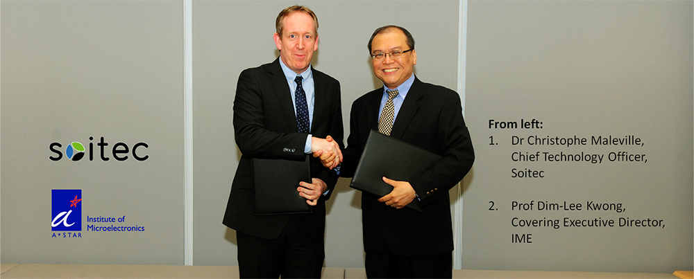
Singapore and Bernin (Grenoble)- March 26- 2019 - The Agency for Science- Technology and Research's (A*STAR) Institute of Microelectronics (IME) and Soitec (Euronext Paris)- a world leader in designing and manufacturing innovative semiconductor materials- announce the launch of a joint program to develop and integrate a new layer transfer process within advanced wafer level multi-chip packaging techniques. Based on the combination of IME's Fan-Out Wafer Level Packaging (FOWLP) and 2.5D Through Silicon Interposer (TSI) technologies with Soitec's Smart Cut™ technology- the new cost competitive process offers higher performance- energy efficiency and increased product yield.
Advanced packaging is used in many of today's systems on chip (SOCs) for servers- high-end mobile- industrial- and automotive applications- and involves various approaches for combining semiconductor chips into packages to reduce costs- improve power efficiency- and provide efficient heat dissipation. By 2022- the advanced packaging market segment is expected to triple to two million wafer starts for mid- to high-end applications. The rising complexity of today's chips with growing numbers of smaller and smaller transistors and circuits requiring high I/O counts is driving collaborative innovation across the advanced packaging process community focused on identifying cost effective solutions for manufacturing- and increased data bandwidth to support hand-held- cloud and edge computing applications.
One of the standard processes in advanced packaging involves using a full silicon wafer for the layer transfer process- which can cost up to 3 cents/mm2. Soitec will partner with IME over the next three years to evaluate the use of its Smart Cut™ technology on IME's advanced packaging platforms FOWLP and 2.5D TSI- with the objective to integrate a new layer transfer process as a key step in future generations of packaging techniques. This new process targets improved performance- lower power consumption and reduced production costs by eliminating the need to consume a full silicon wafer. IME will also conduct tests to evaluate the reliability and robustness of the newly developed process- which will help Soitec to determine its long-term viability.
Smart CutTM technology makes use of both implantation of light ions and wafer bonding to define and transfer ultra-thin single-crystal layers from one substrate to another. It works like an atomic scalpel and allows active layers to be managed independently from the supporting mechanical substrate. Key benefits include the creation of multiple thin nanometric scale layers of virtually defect-free silicon by utilizing low temperature bond and split techniques. These layers are then placed on top of active transistor circuitry. The thickness of the transferred layer can be determined with a high degree of precision by adjusting the implantation energy and process engineering. Transistors can then be completed using etch and deposition processes. Moreover- the donor substrate can be reused many times as the surface of the silicon wafer is repolished after each layer transfer operation- and the substrate can be reused.
As a leading research institute- IME brings together the global semiconductor supply chain- including fabless companies- foundries- OSATs- EDA suppliers- equipment manufacturers- and materials developers to demonstrate advanced packaging solutions for mobile- data-center- high-performance computing- 5G- IoT and automotive applications. Through this collaboration with Soitec- IME will provide advanced packaging expertise in architecture definition- modeling- design- process-integration- reliability-assessment and failure analysis. IME will execute the advanced packaging development in its fully functional- state of the art 300mm wafer level packaging- 2.5D/3DIC pilot line. IME's end-to-end process capabilities and know-how in advanced FOWLP and 2.5D TSI will shorten development cycles and demonstrate cost-effective packaging solutions using Smart CutTM technology. During the joint program- Soitec will contribute significant tool time- R&D personnel- and dedicated space in its clean room at its Pasir Ris fabrication facility in Singapore.
"Advanced packaging continues to be a bright spot in the high-value semiconductor market. We are excited to partner Soitec to develop packaging solutions that will contribute to the dynamic growth of this high-potential segment in Singapore and worldwide-" said Professor Dim-Lee Kwong- Covering Executive Director- IME.
"Soitec and IME believe Smart Cut™ technology will deliver breakthrough results- revolutionizing 2.5D/3D layer transfer process flow-" said Christophe Maleville- Soitec's Chief Technology Officer. "This strategic collaboration will not only develop a new Smart Cut™ application serving new generations of advanced packaging- but also open a brand-new market for Soitec beyond traditional engineered substrate manufacturing."
About A*STAR's Institute of Microelectronics (IME)
The Institute of Microelectronics (IME) is a research institute of the Science and Engineering Research Council of the Agency for Science- Technology and Research (A*STAR). Positioned to bridge the R&D between academia and industry- IME's mission is to add value to Singapore's semiconductor industry by developing strategic competencies- innovative technologies and intellectual property; enabling enterprises to be technologically competitive; and cultivating a technology talent pool to inject new knowledge to the industry. Its key research areas are integrated circuits design- advanced packaging- bioelectronics and medical devices- MEMS- nanoelectronics- and photonics. For more information on IME- please visit www.ime.a-star.edu.sg.
About the Agency for Science- Technology and Research (A*STAR)
The Agency for Science- Technology and Research (A*STAR) is Singapore's lead public sector agency that spearheads economic oriented research to advance scientific discovery and develop innovative technology. Through open innovation- it collaborates with its partners in both the public and private sectors to benefit society.
As a Science and Technology Organization- A*STAR bridges the gap between academia and industry. Its research creates economic growth and jobs for Singapore and enhances lives by contributing to societal benefits such as improving outcomes in healthcare- urban living and sustainability.
A*STAR plays a key role in nurturing and developing a diversity of talent and leaders in its Agency and research entities- the wider research community and industry. A*STAR's R&D activities span biomedical sciences and physical sciences and engineering- with research entities primarily located in Biopolis and Fusionopolis. For ongoing news- please visit www.a-star.edu.sg.
About Soitec
Soitec (Euronext- Tech 40 Paris) is a world leader in designing and manufacturing innovative semiconductor materials. The company uses its unique technologies and semiconductor expertise to serve the electronics markets. With more than 3-000 patents worldwide- Soitec's strategy is based on disruptive innovation to answer its customers' needs for high performance- energy efficiency and cost competitiveness. Soitec has manufacturing facilities- R&D centers and offices in Europe- the U.S. and Asia. Soitec and Smart Cut are registered trademarks of Soitec. For more information- please visit www.soitec.com and follow us on Twitter: @Soitec_EN
Soitec and Smart Cut are registered trademarks of Soitec.
# # #
Soitec is a French joint-stock corporation with a Board of Directors (Société Anonyme à Conseil d'administration) with a share capital of € 62-762-070.50- having its registered office located at Parc Technologique des Fontaines - Chemin des Franques – 38190 Bernin (France)- and registered with the Grenoble Trade and Companies Register under number 384 711 909.
# # #
[1]Source: Yole Development 2017 report for 3D TSV and 2.5D by 12" wafer starts.
Was This Article Helpful ?
A*STAR celebrates International Women's Day

From groundbreaking discoveries to cutting-edge research, our researchers are empowering the next generation of female science, technology, engineering and mathematics (STEM) leaders.
Get inspired by our #WomeninSTEM

