A*STAR NEWS
A*STAR's Inaugural "Innovate Together" Showcases Singapore's Semiconductor Ambitions On Global Stage
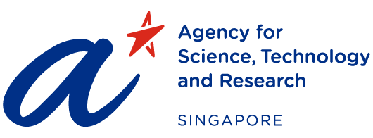
Mr Beh Kian Teik, Chief Executive Officer, A*STAR delivered the opening address at the A*STAR Innovate Together event on 21 May 2025.
New initiatives and global partnerships were unveiled during the inaugural event to strengthen Singapore’s semiconductor capabilities
World’s first industry-grade 200mm Silicon Carbide Open R&D Line launched to accelerate innovation and collaboration for Silicon Carbide devices
Lab-in-Fab 2.0 powering sustainable, efficient and high-performance innovations and high-value manufacturing in piezoelectric MEMS in Singapore
EDA Garage to equip local companies with cost effective advanced design tools, strengthening Singapore’s Integrated Circuit design ecosystem
SINGAPORE – The Agency for Science, Technology and Research (A*STAR) today hosted the inaugural “Innovate Together” event at SEMICON Southeast Asia 2025, signalling Singapore’s bold ambition to lead in the next phase of semiconductor innovation. Designed as a convergence point for industry, academia, and the public sector, Innovate Together unveiled game-changing initiatives, strategic global partnerships, and new research platforms that will strengthen Singapore’s position as a high-value semiconductor R&D and talent hub.
"Singapore's semiconductor ecosystem is built on strong collaborations between public agencies, academia, and industry partners," said Professor Yeo Yee Chia, Deputy Chief Executive (Innovation & Enterprise) at A*STAR. "The Innovate Together event exemplifies our commitment to fostering these partnerships and accelerating innovation to address industry challenges and capture new opportunities in the global semiconductor landscape."
At the heart of Innovate Together was the launch of the world’s first industry-grade 200mm Silicon Carbide Open R&D Line by the A*STAR Institute of Microelectronics (A*STAR IME). Designed to enable joint Silicon Carbide (SiC) innovation between researchers and companies, this pioneering facility will strengthen Singapore's capabilities in wide bandgap semiconductor research and address the future demands for high-power applications.
In addition, A*STAR unveiled two other initiatives that will strengthen Singapore’s semiconductor research and innovation capabilities:
Phase two of Lab-in-Fab, a 200mm R&D and manufacturing line focused on piezoelectric Micro-Electro-Mechanical Systems (piezoMEMS), involving partners STMicroelectronics, ULVAC, and the National University of Singapore. This will leverage Singapore’s strong R&D ecosystem to accelerate the development of new piezoelectric materials and devices.
EDA Garage, an initiative that will provide local companies, especially start-ups and SMEs, with cost effective access to advanced Electronic Design Automation (EDA) tools. This will nurture local semiconductor companies and enable them to innovate faster and better.
More information on these initiatives can be found in Annex A.
Advancing semiconductor talent and technologies through global collaborations
As Singapore deepens its capabilities in semiconductor R&D and manufacturing, A*STAR IME is stepping up to connect with global partners to support the growing demand for skilled talent.
To kickstart international collaborations in semiconductor training and R&D, A*STAR IME signed Memorandums of Understanding (MOUs) with key partners, including the Uzeltexsanoat Association, representing Uzbekistan’s electronics sector, the Singapore Semiconductor Industry Association (SSIA), the Indian Institute of Technology, Kharagpur (IIT KGP), and the Fraunhofer Institute for Electronic Nano Systems ENAS.
These partnerships pave the way for internship programmes, joint research projects, and knowledge exchange through training and knowledge sharing activities.
At the sidelines of the SEMICON Southeast Asia 2025 event, A*STAR also formalised its partnerships with GlobalFoundries and Nearfield Instruments, to expand capabilities in advanced packaging and drive innovation in semiconductor metrology technologies.
Under an MOU, GlobalFoundries will gain access to A*STAR’s advanced R&D facilities, capabilities and technical support for technology development in advanced packaging and workforce skills enhancement. The multi-year research collaboration between A*STAR IME and Nearfield Instruments, a leader in advanced semiconductor metrology, will accelerate the development of advanced metrology solutions that enable efficient chip production.
The Innovate Together event featured expertise from leading institutions on key technological areas that are important for the future of Singapore’s semiconductor industry. Speakers from A*STAR, National University of Singapore (NUS), Nanyang Technological University, Singapore (NTU Singapore), and the National Semiconductor Translation and Innovation Centre (NSTIC) shared the latest insights on advanced packaging, photonics, MEMS, and mmWave and beyond.
Attendees gained valuable perspectives on Singapore's growing capabilities in upcoming semiconductor technologies and the importance of ecosystem collaborations in driving innovation, as well as discussed how collaborative R&D efforts are crucial for addressing complex challenges in semiconductor design, manufacturing, and integration.
– END –
About the Agency for Science, Technology and Research (A*STAR)
The Agency for Science, Technology and Research (A*STAR) is Singapore's lead public sector R&D agency. Through open innovation, we collaborate with our partners in both the public and private sectors to benefit the economy and society. As a Science and Technology Organisation, A*STAR bridges the gap between academia and industry. Our research creates economic growth and jobs for Singapore, and enhances lives by improving societal outcomes in healthcare, urban living, and sustainability. A*STAR plays a key role in nurturing scientific talent and leaders for the wider research community and industry. A*STAR’s R&D activities span biomedical sciences to physical sciences and engineering, with research entities primarily located in Biopolis and Fusionopolis
Annex A – Information On A*star’s Announcements At Innovate Together
Announcement 1: Launch Of 200mm Silicon Carbide Open R&d Line
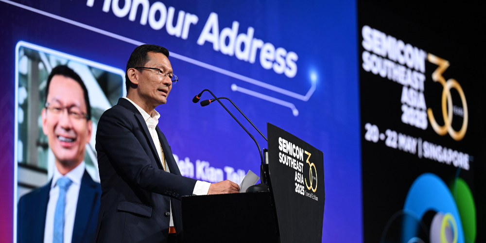
Dr Navab Singh, Deputy Executive Director of Research at the A*STAR Institute of Microelectronics, shared about the world’s first industry-grade 200mm Silicon Carbide Open R&D Line during the A*STAR Innovate Together event on 21 May 2025.
A*STAR Institute of Microelectronics (A*STAR IME) has launched the world’s first industry-grade 200mm Silicon Carbide Open R&D Line to enable and accelerate Silicon Carbide (SiC) innovation from materials growth and defect analysis to device fabrication and testing.
The Open R&D Line addresses key challenges faced in the development of SiC devices, including high cost of industry-grade tools, limited access to advanced technologies, complex and fragmented development processes, and lack of collaboration and knowledge sharing.
How The Industry Can Benefit
By offering a complete suite of SiC development and pilot manufacturing capabilities under one roof, the Open R&D Line increases the speed of R&D by eliminating the fragmented R&D processes that previously required researchers and companies to work with multiple facilities.
The Open R&D Line enables the development of advanced technologies by having a close partnership with key equipment OEMs and materials suppliers—ASM, centrotherm, Nissin, Soitec and Toray—who have contributed their latest technologies and are co-developing their next-generation products with A*STAR:
ASM’s PE1O8 tool for depositing high-quality SiC epitaxial layers
centrotherm’s c.ACTIVATOR 200 and c.OXIDATOR 200 tools for high-temperature SiC annealing and oxidation
Nissin’s first and only in-situ X-ray diffraction capability for the SiC ion implantation process
Soitec’s SmartSiCTM semiconductor engineered substrate technology
Toray’s innovative materials for SiC power module packaging products
While it was being established, the Open R&D Line has already demonstrated its value to the semiconductor industry. Several global and local companies have partnered with A*STAR IME to utilise its capabilities, highlighting strong industry demand for such collaborative platforms:
STMicroelectronics is leveraging engineering capabilities and tools to develop ways to streamline its manufacturing processes and improve the quality of its SiC devices
One of the top foundries in the world is developing key process technologies through the Open R&D Line, with the intention to scale up production of advanced SiC devices
WaferLead, a local start-up, is using the Open R&D Line to develop, evaluate, and enhance the performance and reliability of its wafers
Announcement 2: Launch Of Lab-in-fab Phase Two
Mr Bertrand Stoltz, STMicroelectronics’ Executive Vice President, Corporate Finance, Asia Public Affairs, Managing Director Singapore, spoke about the Lab-in-Fab phase two collaboration between A*STAR, STMicroelectronics, ULVAC and the National University of Singapore during the A*STAR Innovate Together event on 21 May 2025.
A*STAR Institute of Microelectronics (A*STAR IME), STMicroelectronics and ULVAC have announced phase two of their “Lab-in-Fab” initiative, a 200mm R&D and manufacturing line in Singapore that is focused on piezoelectric Micro-Electro-Mechanical Systems (piezoMEMS) technology. This collaboration combines STMicroelectronics’ expertise in piezoMEMS R&D and wafer manufacturing, ULVAC’s advanced manufacturing equipment, and A*STAR IME’s expertise in piezoelectric thin film materials and device design.
Lab-in-Fab is positioned to become a catalyst for innovation, bringing together a diverse ecosystem of sensor and actuator design companies, product companies as well as manufacturing companies and their suppliers, to collaboratively prototype and manufacture new products for various applications. To date, it has commercialised new lead-free piezoelectric materials and device platforms, as well as created employment opportunities in Singapore. Additionally, Institutes of Higher Learning from Singapore and globally have tapped on Lab-in-Fab for their research and training needs.
The second phase of Lab-in-Fab expands the partnership to include A*STAR Institute of Materials Research and Engineering and the National University of Singapore, to further accelerate the development of new piezoelectric materials and devices. It also adds sustainability as a central focus, to develop more energy efficient lead-free piezoMEMS transducers using environmentally friendly materials like scandium-doped aluminium nitride (ScAIN).
Outcomes of Lab-inFab Phase One
Beyond technology development, Lab-in-Fab phase one introduced a Multi-Wafer Project (MPW) service for local and international universities and institutes, enabling new innovations for piezoMEMS devices and applications. This service will continue to provide differentiated piezoMEMS platforms that accelerate innovation for both researchers and companies.
Local SMEs have gained new capabilities through their participation in Lab-in-Fab. Micronclean, a local SME providing cleanroom services in Singapore, has developed a decontamination protocol that meets high-volume foundry requirements, strengthening its technical capabilities and expanding its business opportunities.
ANNOUNCEMENT 3: LAUNCH OF EDA GARAGE
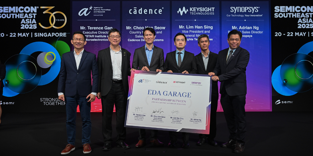
(Left to right) Mr Beh Kian Teik, Chief Executive Officer, A*STAR; Mr Terence Gan, Executive Director, A*STAR Institute of Microelectronics; Mr Seow Choo Han, Country Manager and Sales Director for Singapore, Cadence; Mr Lim Han Sing, Vice President and General Manager for General Electronics Measurement Solutions (GEMS) of the Electronic Industrial Solutions Group, Keysight; Mr Soh Leng Wan, Assistant Managing Director, Enterprise Singapore; and Mr Adrian Ng, Regional Sales Director for Southeast Asia, Synopsys during the launch of the EDA Garage on 21 May 2025.
To make advanced Electronic Design Automation (EDA) tools accessible to local companies, especially start-ups and SMEs, the A*STAR Institute of Microelectronics (A*STAR IME), Enterprise Singapore, and EDA companies—Cadence, Keysight, and Synopsys—have come together to establish the EDA Garage.
EDA tools are specialised software suites that are used to design, simulate, analyse and verify semiconductor chips virtually before they are fabricated. These tools help to ensure that the designed chips meet performance requirements, while eliminating errors in the design process.
Under the EDA Garage, local companies will be able to purchase flexible, pay-per-use tool licenses. In addition, Cadence, Keysight and Synopsys will offer training and support to use their tools. This lowers the barrier to entry for companies who are designing their first chips.
This initiative aims to nurture local semiconductor companies, and enable new innovations. The support by EDA companies will also contribute to building a skilled workforce, further strengthening Singapore's competitiveness in the global semiconductor industry.
CM Engineering Labs Singapore, a local company which develops radio frequency and analog integrated circuits for wireless communication and sensing applications, is the first subscriber of the EDA Garage.
Key Features of the EDA Garage
License Hosting: A*STAR IME will host all EDA tool licenses on servers for EDA Garage, ensuring seamless access for participating companies.
Dedicated Setup: Each participating company will be assigned a dedicated server for design computation and database storage, as well as desktops.
Design Hardware and Data Backup: Essential IC design tools will be provided, along with data backup services to prevent data loss and ensure compliance with audit requirements.
ANNEX B – List of speakers at Innovate Together
ADVANCED PACKAGING
Prof Lim Yeow Kheng, Assistant Dean, Research and Technology, College of Design and Engineering, National University of Singapore
Mr Vempati Srinivasa Rao, Director, Heterogeneous Integration, A*STAR Institute of Microelectronics (A*STAR IME)
PHOTONICS
Assistant Prof Brian Sia, School of Electrical & Electronic Engineering, Nanyang Technological University, Singapore
Prof Ang Kah Wee, Chief Technology Officer, National Semiconductor Translation and Innovation Centre (NSTIC)
MEMS
Dr Zhu Yao, Head of Department, MEMS, A*STAR Institute of Microelectronics (A*STAR IME)
MMWAVE AND BEYOND
Prof Ng Geok Ing, Executive Director, National Gallium Nitride Technology Centre

Was This Article Helpful ?
A*STAR celebrates International Women's Day

From groundbreaking discoveries to cutting-edge research, our researchers are empowering the next generation of female science, technology, engineering and mathematics (STEM) leaders.
Get inspired by our #WomeninSTEM