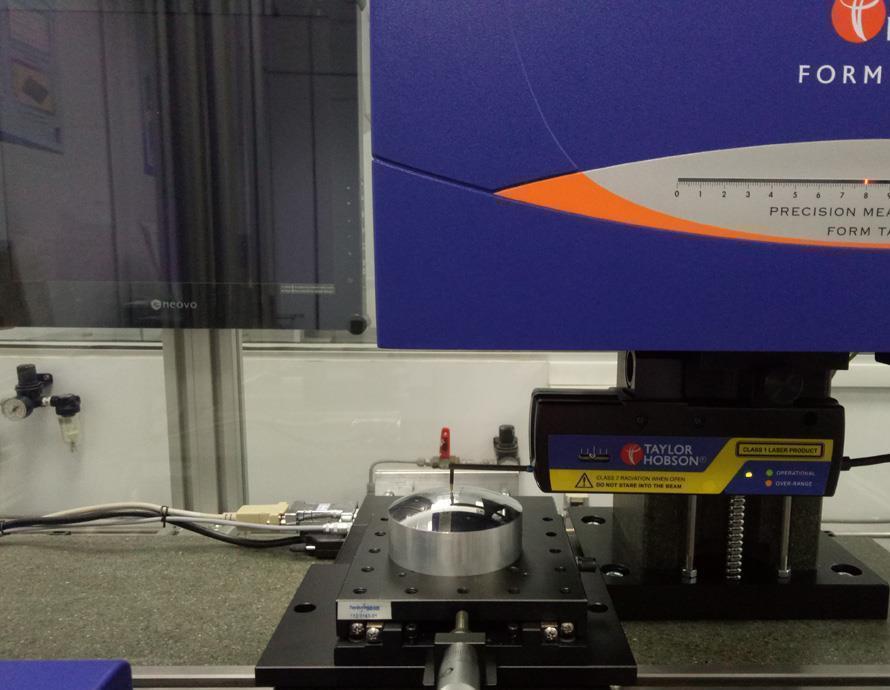
Stylus Profilometer

stylus-profilometer

Interested to Know More?

Probe-based profiler capable of 3D surface profilometry and surface roughness characterization at nanometer level.


EQUIPMENT SPECIFICATIONS
    There are multiple stylus profilometers available:
  • Model: Form Talysurf 200
    • Vertical resolution: 0.2 nm
    • Data sampling in X-axis: 0.125 µm
    • Max. scan size: 200 mm (x) x 100 mm (y) x 25 mm (z)

  • Model: KLA Tencor P16
    • Wafer Size: From small samples up to 200mm wafers
    • Scan range: up to 200 mm
    • Vertical range: up to 110 um
    • Step height repeatability of 6Å or 0.1% (1σ)

  • Model: Talylor Hobson PGI2540
    • Measuring range:
      • Z axis – 12.5 mm ( 60 mm stylus arm), 25.0 mm (120 mm stylus arm)
      • X axis – 200 mm
    • Measuring resolution:
      • Z axis – 0.2 nm at 12.5 mm range, 0.4 nm at 25.0 mm range
      • X axis – 125 nm over 200 mm
    • System noise: 1 nm RMS
    • Form measuring uncertainty: 200 nm
    • Stylus radius: 2 µm, 5 µm, 0.25 mm and 0.5 mm

  • Model: Panasonic UA3P
    • Direct traceability to SI metre
    • Measuring range: 30 mm x 30 mm x 20 mm
    • Measuring resolution: 3 nm
    • Maximum measuring angle: 75 °
    • Measuring uncertainty:
      • Less than 30°: 50 nm
      • 30°to 45° : 80 nm
      • Above 45° : 150 nm
    • Stylus Radius: 2 μm (Diamond), 0.5 mm (Ruby)
    • Probing force : 150 to 300 μN

  • Model: NanoMap-500LS 3D Contact Surface Profilometer
    • Piezo Tip scan
    • Z range: nm to 1m
    • XY scanning range: up to 150X150mm
    • Generates both 3D image and 2D images
    • Integrated color optical camera for direct sample viewing during scanning


CAPABILITIES / APPLICATIONS
High-precision measurement on machined parts or coatings with high surface quality for manufacturing industry in precision engineering, optics, electronics, etc.


LOCATION
V1-E06b, SIMTech Valley Block (Level 1)
73 Nanyang Dr, Singapore 637662

National Metrology Centre
1 Science Park Dr, Singapore 118221

Institute of Materials Research and Engineering
Synthesis, 6 Fusionopolis Link

Institute of Microelectronics
11, Science Park Road, Singapore Science Park II, Singapore 117685


EQUIPMENT ENQUIRY