
A*STAR NEWS
Innovation - The Essential Bargaining Chip
As society demands smaller- swifter and smarter devices- microchip manufacturers are seeking novel methods to scale up functionality while keeping costs low.
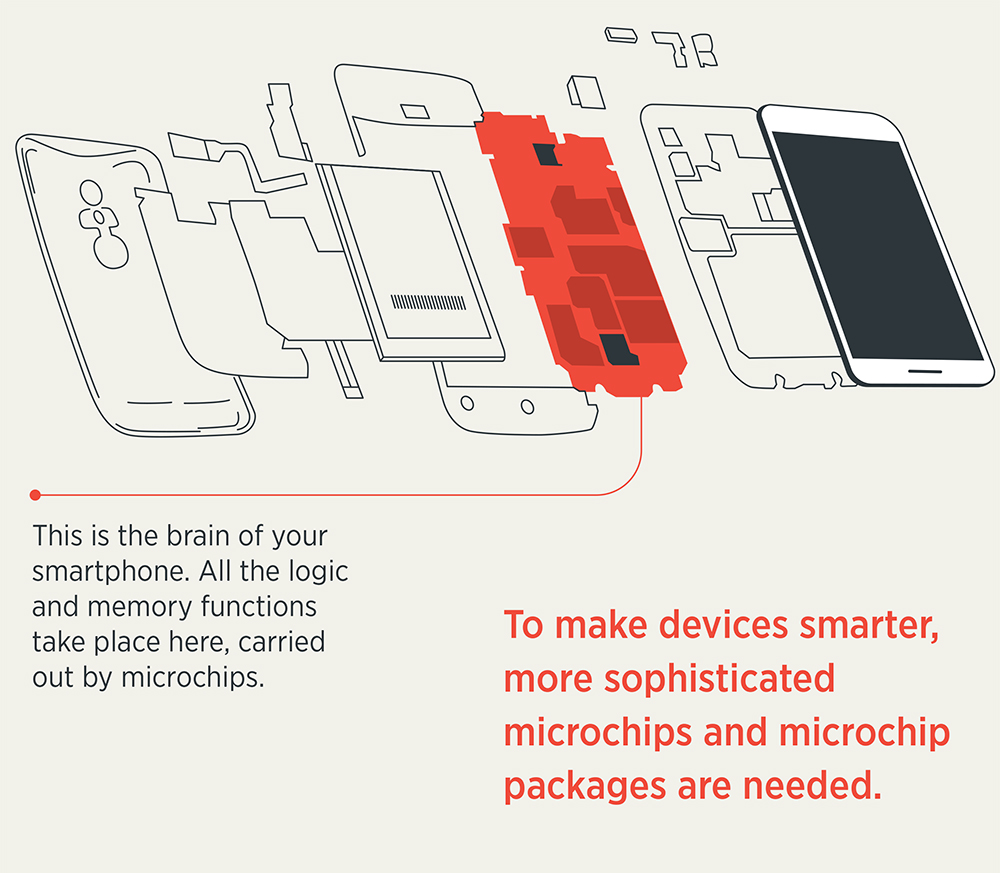
Pause for a moment to marvel at the feat of engineering that is your smartphone. Personal computing has certainly come a long way from the huge mainframes of the 1960s- to the desktops of 1990s to the pocket-sized devices we now carry around – all of which are made possible by microchip technology.
Like brains that process information and retain memories- microchips carry out calculations and store data integrated circuits (ICs). Their speed and capacity to perform logic and memory tasks depend on the number of transistors installed within. In 1965- Gordon Moore- co-founder and chairman emeritus of Intel Corporation- forecast that the number of transistors on a silicon chip would double every two years. Moore’s law- as it came to be known- has held true over the last five decades- resulting in ever-shrinking microchips and increasingly multi-functional devices.
While this doubling strategy of ‘more Moore’ has served society well- its limitations are also beginning to show. For instance- the cost of increasing transistor density within microchips is becoming prohibitive. “You cannot pack any more of these transistors into a silicon chip economically-” said Dr Surya Bhattacharya- Director of System in Package- Interconnect and Packaging Program at the Institute of Microelectronics (IME)- Agency for Science- Technology and Research (A*STAR). "Today- companies are working to make chips with dimensions as small as 7 nm- but those are really expensive- and few companies can afford it."
Form and function
No stranger to the field of microelectronics- Bhattacharya has over 25 years of experience in the semiconductor technology industry. He started out his career as a technology manager in the semiconductor industry during the dot-com boom. He eventually rose to the position of Director of Foundry Engineering at telecommunications equipment company Qualcomm- overseeing its technology and manufacturing ramps across foundries in Asia and around the world. He took up his current position at IME in 2011- bringing his technical expertise and commercial savvy to the research institute.
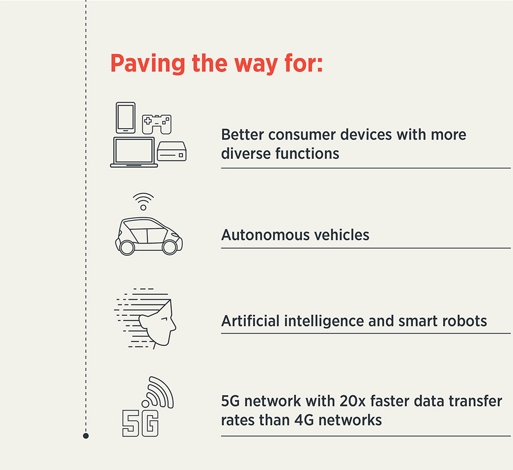
Bhattacharya noted that society still demands more from the microchip. From artificial intelligence that promises to revolutionise business data analytics- to autonomous vehicles that raise the possibility of effortless commuting and safer roads- all these emerging technologies rely on the creation of more sophisticated microchips that pack greater functionality into a compact form factor- while remaining cheap to produce.
While this appears to be a tall order given the high cost of raising transistor density- semiconductor industry players have risen to the challenge with advanced packaging methods. "Advanced packaging allows memory and logic chips to be placed inside a single package- creating a multi-chip package- or a system-in-package-” said Bhattacharya. “In this case- you don’t need to depend entirely on transistor scaling to add on new functions and improve performance; you can achieve the same goal using a modular approach—through system scaling."
Fanning the flames of innovation
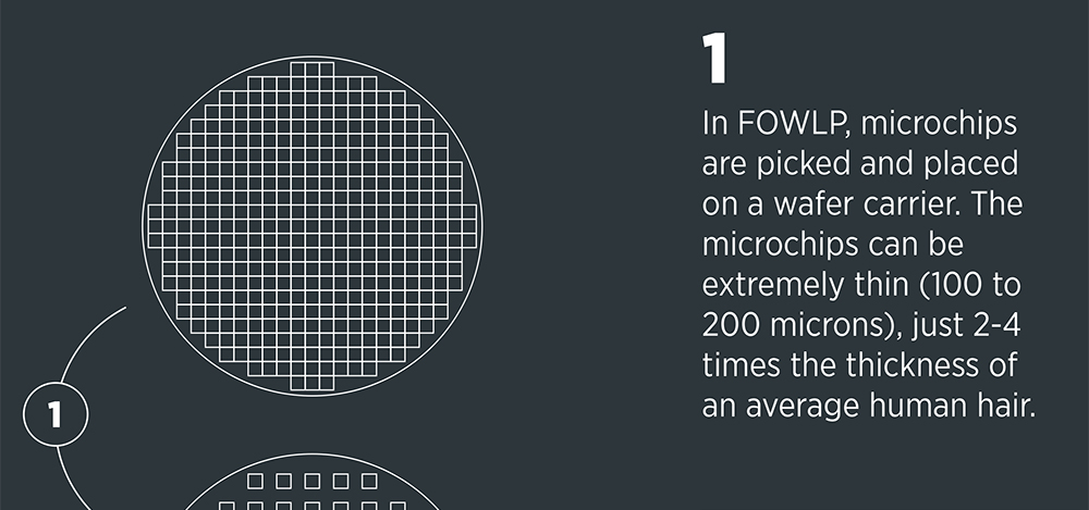
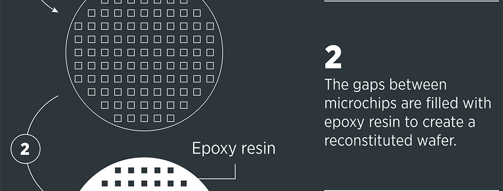
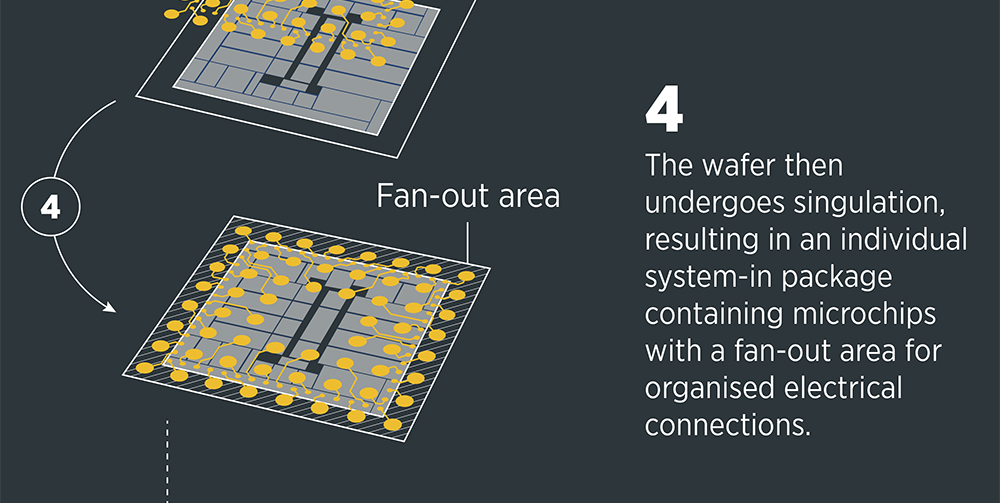
A cost-efficient method to achieve system scaling is fan-out wafer-level packaging (FOWLP). The process begins with individual chips being embedded in an epoxy layer to form a wafer—think of this as raisins placed at regular intervals on a thin- flat piece of dough. The dough is then baked so that it solidifies- and the raisins are sealed in place.
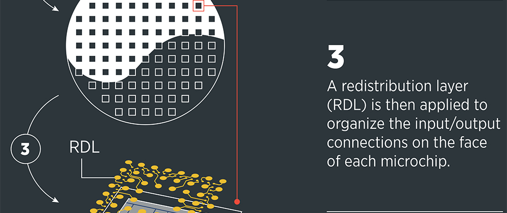
Next- imagine a pattern of icing being applied to the dough—analogous to the redistribution layer that organises the thousands of connections found on the face of each chip into a specific configuration. “Importantly- because there is an epoxy-filled space between the microchips [the dough between the raisins]- each chip’s connections can be distributed beyond the confines of the chip itself- allowing for more connections. These connections ‘fan out’ from each chip- thus giving the FOWLP technique its name-” said Dr Yoon Seung Wook- Director- Group Technology Strategy- at semiconductor solutions provider STATS ChipPAC Pte. Ltd.- a member of JCET Group.
Thereafter- the dough is sliced up so a single raisin rests on each piece. This corresponds to the singulation step in FOWLP- whereby the wafer is divided into discrete packages. “With FOWLP- you can process the entire reconstituted wafer at the same time rather than do it for individual chips- so it’s a very powerful and efficient technique-” Bhattacharya explained.
IME- together with STATS ChipPac- helped pioneer the development of high-density FOWLP in Singapore. The collaboration between the two parties resulted in an optimised workflow for the creation of sophisticated chip packages supporting a multitude of industrial and consumer electronic devices- including the smartphone you hold in your hand.
Foundations for 5G
Keeping pace with society’s yearning for smarter devices is its need for faster internet. A minute spent downloading a high-resolution movie is a minute too long; these days- patience wears thin in seconds. Under these circumstances- 5G networks- which promise 20-times faster data transfer rates than current 4G networks and 100-fold greater mobile data volume- could not come sooner.
Movie buffs aren’t the only ones eagerly anticipating the advent of 5G networks. Roboticists and self-driving vehicle manufacturers also require rapid data transfer so that their fleets of autonomous androids or cars can to ‘talk’ to one another and respond to dynamic environments in real time. In short- 5G could revolutionize the way people interact with machines and the digital world.
Because 5G networks operate in the millimetre wave band between 30 and 300 gigahertz- antennas that can transmit and receive signals at those radio frequencies must be packaged with other wireless communication elements. Unlike the long antennas of old- millimetre wave antennas are tiny- with dimensions in the millimetre range- and can be integrated as an array in a chipset via FOWLP. However- to optimise the process and make it practical for widespread industrial use- a deeper understanding of fundamental physical principles and materials science is needed.
“As a solutions provider in the semiconductor industry- we are very much focused on product development. Hence- we need scientists at research institutes such as IME to help fill our knowledge gaps in science and engineering- which can then be applied to improve advanced packaging. This will eventually lead to next-generation connected devices with greater functionality-” said Yoon.
“Moore’s law has no doubt set the foundation for technological innovations and breakthroughs in our modern devices. But we have come to learn that its economic limitations force the industry to find new ways to work around it- so as to support faster- smarter and more complex devices in a new era of innovation. We aim to do this with our industry partners; and with the setup of IME’s full FOWLP development line- we can quicken the development of novel advanced packaging techniques- to keep up with rapidly evolving trends-” Bhattacharya concluded.
By harmonising theory and practice- faster and more power-efficient data centres- artificial intelligence-enabled smartphones- self-driving cars and faster 5G internet with innovative chip packaging technologies- could become a reality sooner than later – all enabled by the evolving chip of the future.
For more information on FOWLP and collaboration opportunities with IME- please email Dr Surya Bhattacharya at bhattass@ime.edu.sg
Was This Article Helpful ?
A*STAR celebrates International Women's Day

From groundbreaking discoveries to cutting-edge research, our researchers are empowering the next generation of female science, technology, engineering and mathematics (STEM) leaders.
Get inspired by our #WomeninSTEM