Powering greener transport: How WaferLead’s silicon carbide wafers drive efficiency in EVs and beyond
Jump to Section: The Challenge | Our Innovation | The Impact

Transport generates 37 per cent of global carbon emissions, making its transformation critical in tackling climate change. One promising solution is electric vehicles (EVs) but their success depends on a hidden component: semiconductor wafers.
While traditional silicon wafers work, their inability to handle high voltages, temperatures, and heat well means devices that use them need to be bigger, thicker, and have larger cooling systems. The result is heavier and less efficient EVs.
Singapore startup WaferLead set out to change this in 2019 by developing superior silicon carbide (SiC) wafers that overcome these issues. The endeavour was made possible by A*STAR’s Technology for Enterprise Capability Upgrading (T-Up) programme, which provides local firms access to skilled scientists and research engineers for up to two years to aid in research and development (R&D).
Today, WaferLead, a T-Up Excellence Awards 2025 finalist, is enabling semiconductor manufacturers across the world from AppliedSiC in the US to ArchLab in South Korea, to develop smaller, lighter, and more energy-efficient devices.
The Challenge
SiC power modules are 45 per cent smaller, 40 per cent lighter, and 5 to 10 per cent more energy-efficient than silicon ones. For EVs, this could mean travelling 120km instead of 100km on a single charge, a 20 per cent boost in mileage that could accelerate EV adoption. 3 However, growing SiC crystals invariably produces defects that can cause transistors which control electrical current flow in semiconductors to fail, reducing device yields and increasing costs. To address this, manufacturers add an epitaxial layer — an additional SiC coating that minimises surface defects.
Here’s the catch: higher-voltage applications like EVs require proportionally thicker epitaxial layers for better insulation, but thicker layers typically introduce more defects.
WaferLead’s Chief Executive Officer and former A*STARResearcher, Dr Sunil Wickramanayaka, knew a novel manufacturing process was long overdue but he needed a scientist with a deep understanding of semiconductor manufacturing to create one. While he could train a member of his team or hire someone new, this would have been costly and time-consuming. So he turned to A*STAR’s T-Up programme
Our Innovation
Drawing on more than a decade at A*STAR’s Institute of Microelectronics (IME) and a wealth of expertise in semiconductor manufacturing, Dr Xie Ling has been instrumental to WaferLead since stepping in as a technical advisor in 2023.

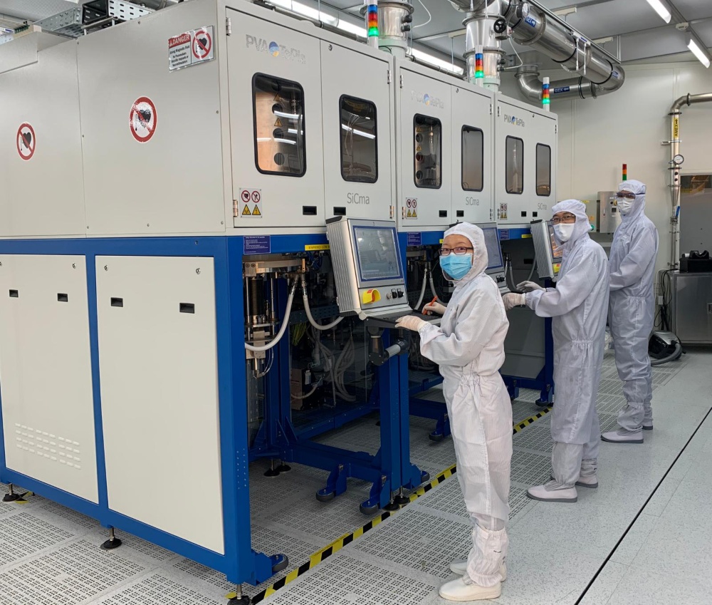
Dr Xie Ling (front) and Waferlead staff running crystal growth furnaces.
Her expertise in chemical vapour deposition, the process by which an epitaxial layer can be deposited on the base wafer, enabled WaferLead to break through long-standing manufacturing process challenges. The result: improved epitaxial SiC wafer production through uniform temperature control, precise particle management, and optimised source materials.
Key contributions from A*STAR included:
- Tracing the origins of defects and devising targeted defect prevention strategies. This resulted in proprietary recipes that enabled the deposition of epitaxial layers up to 90 micrometres thick with extremely low defect densities.
- An accelerated R&D process, which took just three months with the help of Dr Xie and the T-Up programme, instead of a year if done from scratch.
Besides technical research, I was exposed to the business side of WaferLead — how the company operates, communicates with customers, and makes deals. It was an eye-opening experience, which I would not have gained if I had stayed within my comfort zone at A*STAR.
— Dr Xie Ling, A*STAR researcher and T-Up participant
The Impact
WaferLead has established itself as a leading player in the global electronics market with three key achievements:
- Business growth: : WaferLead sold US$480 million worth of bare and epitaxial SiC wafers in 2024. Its revenue for 2025 is forecast to be between S$800,000 and S$1 million, with over US$400 million (S$513 million) in secured investments for future production facilities.
- Technical excellence: By keeping defect densities below 0.2 per sq cm, it is able to bump up device yields to above 80 per cent. This can command a 20 to 30 per cent price premium over competitors’ products.
- Energy savings: SiC adoption saves up to 10 per cent more in electricity consumption compared with silicon. This helps numerous industries, from EV manufacturers to computer game makers, become greener.
If you look at the switch from silicon to silicon carbide devices, the main plus point is that you consume five to 10 per cent less power. Apply that to a power station and it reduces energy loss during the power conversion process. So if it has a capacity of 10 megawatt of energy, you will be saving one megawatt of power — which is significant.
— Dr Sunil Wickramanayaka, Chief Executive Officer and Founder of WaferLead
The company is now working to establish an SiC wafer pilot production line in Singapore, as well as a high-volume production line in Europe and India. As energy demand continues to rise, WaferLead is not only helping to strengthen the world’s deep-tech capabilities, but also making it more sustainable in the process.
A*STAR celebrates International Women's Day

From groundbreaking discoveries to cutting-edge research, our researchers are empowering the next generation of female science, technology, engineering and mathematics (STEM) leaders.
Get inspired by our #WomeninSTEM


