A*STAR IMRE’s R&D Opens an Avenue for Wafer-Scale 2D Semiconductors
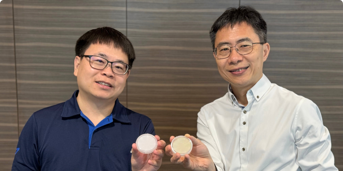 Lead author Dr Fu Wei and Principal Investigator Prof Johnson Goh showing a typical untreated sapphire wafer (left) and the successful 2D semiconductor film with oriented crystal domains grown on their surface engineered sapphire substrate (right)
Researchers at A*STAR’s Institute of Materials Research and Engineering (A*STAR IMRE) have achieved a significant breakthrough in the scalable fabrication of 2D semiconductors.
While epitaxial growth of 2D semiconductors is supposed to be guided by the underlying atomic order in the sapphire substrate, large-area growth has often resulted in randomly oriented polycrystalline structures. This limitation has posed a major challenge for the reproducibility and scalability of 2D quantum materials.
Led by Dr Fu Wei (Lead Author) and Prof Johnson Goh (Principal Investigator), the A*STAR IMRE team uncovered a key degradation mechanism in sapphire substrates - hydrolysis triggered by moisture exposure - that disrupts the atomic order necessary for aligned crystal growth. This issue is particularly pronounced in humid environments such as Singapore, where unintentional contact with moisture during transport or handling can gradually disorder the pristine alumina surface of sapphire. Through systematic ageing studies, the team demonstrated how hydrolysis leads to crystal misorientation and developed effective countermeasures to restore surface integrity.

These innovations enabled the reproducible growth of single-orientation 2D tungsten sulphide (WS₂) across wafer scale, dramatically improving device yield from a few percent (typical of hand-exfoliated flakes) to over 95%. This advancement marks a critical step in translating 2D materials from lab-scale novelty to scalable engineering platforms for optoelectronic and quantum applications.
The study was supported by A*STAR IMRE’s advanced materials characterisation capabilities, including XPS, RHEED, HRTEM, AFM, and optical techniques. Special recognition goes to Dr Chai Jian Wei, Dr Fabio Bussolotti, and Dr Zhang Mingsheng for working with Dr Fu Wei and Prof Johnson Goh on developing a novel XPS-based analysis method tailored for this project which could have wider applications for the community. The team also acknowledges valuable contributions from collaborators at IHPC, Q.InC, NUS, and former colleague Henry Medina (now at IMEC), who pioneered one of our early techniques to counter the effect of sapphire hydrolysis.
At A*STAR IMRE, materials matter. Here, we put another foot forward for 2D quantum materials.
To learn more about this breakthrough in 2D semiconductor growth, read the full article in Nature Communications:
🔗 https://www.nature.com/articles/s41467-025-63452-9