Applied Materials (AMAT)
In 2011, A*STAR’s Institute of Microelectronics (IME) and AMAT jointly set up a Centre of Excellence in Advanced Packaging in Singapore. Since then, this advanced packaging collaboration has helped build Singapore’s globally competitive advanced packaging capabilities, created new jobs and developed the local ecosystem.

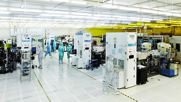
The world-class facility at Singapore’s Science Park II features a 14,000 square foot cleanroom with state-of-the-art semiconductor process equipment custom designed and built by AMAT.
Source: AMAT
Highlights:
- This first-of-its-kind joint lab introduced new capabilities in 3D chip packaging, a critical growth area for the semiconductor industry that will enable the production of smaller and more powerful mobile devices
- In 2016, IME and AMAT extended their research collaboration for five years to focus on advancing key innovations in Fan-Out Wafer-Level Packaging (FOWLP)
- Between 2011 and 2021, the joint lab created over 100 high-value R&D jobs for researchers, scientists and engineers
- Currently, AMAT engages with more than 30 local enterprises in areas such as metrology, machining and fabrication
A*STAR celebrates International Women's Day

From groundbreaking discoveries to cutting-edge research, our researchers are empowering the next generation of female science, technology, engineering and mathematics (STEM) leaders.
Get inspired by our #WomeninSTEM
