I²R Research Highlights
Charting the Future of Semiconductor Inspection with Refined Machine Learning Techniques
The Path to Perfection in Semiconductor Inspection
Inspection and metrology are important in the semiconductor manufacturing process. Accurate and fast inspection established at critical points of the process will ensure that yield can be controlled and maintained.
Aiming to perfect inspection and defect detection in the semiconductor manufacturing process, the Institute for Infocomm Research (I2R)'s recent research paper titled “Improved Bump Detection and Defect Identification for HBMs using Refined Machine Learning Approach,” epitomised the significant advancement in semiconductor inspection, focusing on the essential areas of 2D-3D metrology. Built upon earlier efforts, it introduces a cost-effective, non-destructive approach that employs deep learning and 3D X-ray microscopy for defect detection in the High Bandwidth Memory (HBM) domain.
This paper was awarded the Electronics Packaging Technology Conference (EPTC) 2022 Best Academic Paper Award.
A Deep Dive into the Technology
This breakthrough offers practical solutions to long-standing challenges in the semiconductor industry. The transition to smaller process nodes, from 7nm to 5nm and eventually to 3nm has played a crucial role in driving innovation in the electronics industry, allowing for the development of more powerful and energy-efficient devices. However, it also presents technical challenges, such as increased manufacturing complexity, metrology, and inspection of smaller structures to ensure the quality and reliability of the chips.
This transition has led to a higher defect rate and lower yields in the manufacturing process, further complicating the task of accurately identifying and measuring internal defects like void structures and component misalignments in both 2D and 3D scans. These challenges are compounded by the complex nature of embedded components and the scarcity of data annotation. By utilising advanced machine learning algorithms alongside 3D X-ray microscopy, the team has developed a reliable and effective method for accurately identifying and segmenting embedded defects in semiconductor packaging.
A Closer Look into Methodology
Each 3D scan comprises of 1000 x 1000 x 1000 voxels (each voxel can be thought of as a 3D pixel), amounting to one billion voxels. This immense volume makes it challenging for existing methods to process the data accurately and efficiently. In response, the team divided the problem into two distinct phases: 3D object detection followed by 3D segmentation leveraging on domain knowledge, thus reducing the processing needs for inspecting a chip by up to 80%.
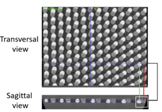
The team adopted a “slice-and-fuse” approach for bump extraction. This involved processing each sagittal slice of the sample with a 2D object detector and then concatenating the results into a 3D bounding box. This technique was especially effective in identifying defective bumps, a notable challenge with prior methods.

Figure 1 One defective sample shown from both transversal and sagittal view
To tackle the imbalanced, “long-tail” distribution of classes in segmentation, the team introduced a combination of weighted criteria and enhancing the training process for imbalanced data. They also compared different differentiable activation functions to optimise the model's generalisability and robustness, resulting in substantial improvements in defect detection and segmentation performance.
Impact and Future Prospects
This research significantly boosts the reliability and efficiency of automatic inspections in semiconductor manufacturing. Looking forward, the team plans to expand their detection approach to barely-supervised learning, aiming to improve the method's applicability and further reduce labelled data requirements. Additionally, efforts are underway to enhance component segmentation, leveraging the recent advancements in the large unified SAM model.
Read more about the paper “Improved Bump Detection and Defect Identification for HBMs using Refined Machine Learning Approach" here.
A*STAR celebrates International Women's Day

From groundbreaking discoveries to cutting-edge research, our researchers are empowering the next generation of female science, technology, engineering and mathematics (STEM) leaders.
Get inspired by our #WomeninSTEM
