The Advanced Nanoanalysis research area in ACI specializes in developing and applying advanced Transmission Electron Microscopy (TEM) techniques to explore the physical and chemical properties of materials at the nano and atomic scales. We offer comprehensive TEM analysis across a wide variety of materials, including those exposed to extreme conditions such as high temperatures and cryogenic environments. Additionally, our lab investigates material dynamics using in situ capabilities with liquid and gas environments. These cutting-edge capabilities open up new possibilities for breakthroughs in fields such as energy storage, catalysis, and next-generation electronics.
Our TEMS
- Sub-atomic analysis from -170 °C to 1000 °C
- Analysis performed in vacuum, liquid, and gas environment
- Ultrafast imaging & mapping with minimum damage to samples with adjustable electron voltage and beam intensity
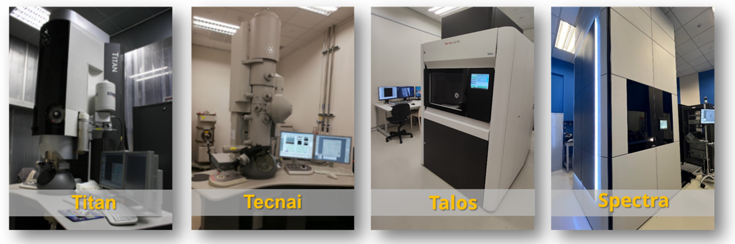
Specifications of TEMs
| TEM | Titan | Tecnal | Talos | Spectra |
| Year | 2006 | 2008 | 2023 | 2024 |
| Electron gun | field emission gun with monochromator 80, 200, 300 KV | field emission gun 200 KV | High-brightness field emission gun 80, 200 KV | High-brightness field emission gun with monochromator 30, 60, 80, 200, 300 KV |
| Resolution | 0.09nm (TEM) 0.10nm (STEM HAADF) | 0.14 nm (TEM) 0.19 nm (STEM HAADF) | 0.12 nm (TEM) 0.16 nm (STEM HAADF) | 0.06 nm (TEM) 0.05 nm (STEM HAADF) |
| Spectroscopy | EDS: solid angle 0.3 sr EELS: Tridiem | EDS: solid angle 1.1 sr EELS: Quantum | EDS: solid angle 0.9 sr | EDS: solid angle 1.8 sr EELS: Continuum |
| Camera | 4k x 4k CMOS | 2k x 2k CCD | 4k x 4k CMOS | 4k x 4k CMOS |
Capabilities
Advanced Transmission Electron Microscopy (TEM)
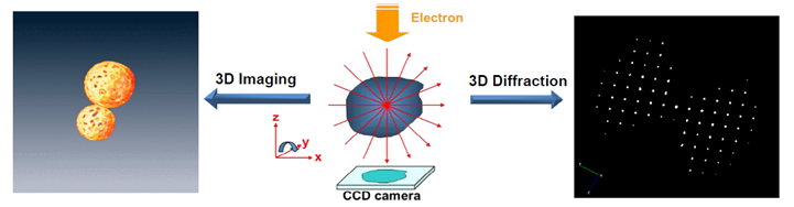
- Obtain 3D morphological and structural information: TEM and STEM tomography & 3D diffraction (MicroED)
- Show amplitude and phase distributions: Electron Holography
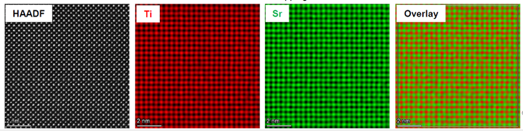
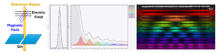
- Achieve high resolution elemental and energy distribution: Monochromated Electron Energy Loss Spectroscopy (EELS), Atomic resolution EDS / EELS mapping
- Provide quantitatively structural information down to nm scale: precession Nano Beam Diffraction and Phase/Crystallographic Orientation Mapping
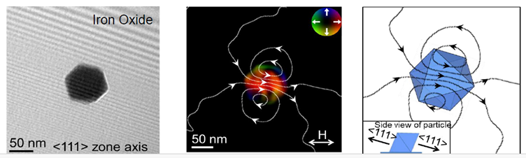
- Visualize magnetic domains and domain walls: Lorentz TEM
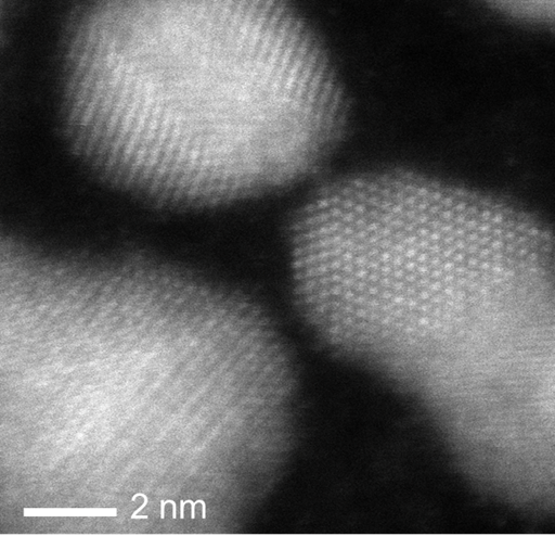
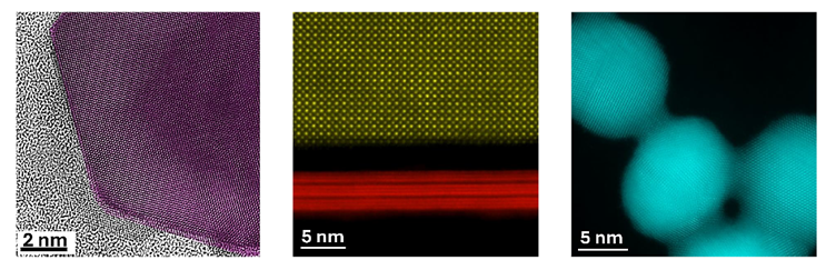 High resolution TEM image of a Te nanowire cross-section (left); Atomic resolution STEM image of SrTiO3 and a layered structure of MoTe2 (centre); Atomic resolution STEM image showing the fusing of Au nanoparticles (right).