The emergence of 2D materials and 2D metamaterials brings exciting opportunities to optoelectronics. The optoelectronics group aims to develop breakthrough technologies by integrating active materials including 2D materials with 2D metamaterials for applications in optical sensing, imaging, communication and computing in wavelength range from DUV to far IR & THz. The key focus areas are: 1) Super resolution focusing and imaging; 2) Mid-far IR transceivers and integrated optoelectronic chip; 3) Optical technology for chemical and physical sensing.
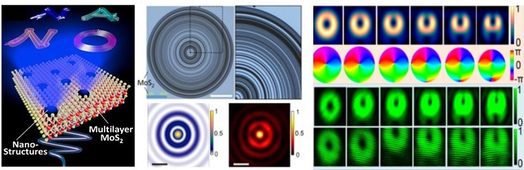
Nano-Photon sieves are developed for holography (left), sub-diffraction limit focusing and imaging (middle), and versatile optical vortex beam generation with integer and fractional orbital angular momentum (right).
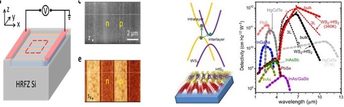
Various mid-far-IR and THz components have been developed, e.g. tunable flat metasurface for complete antireflection in THz (left), high efficiency room temperature operated mid-IR photodetector (right), and THz emitter, polarizer, 2DEG detector, compact optical switch, and tunable plasmonics in THz, etc.
Besides user inspired basic research, we are also collaborating with industry on developing integrated optoelectronics for sensing and imaging applications.