Connect with us

Spin Technology for Electronic Devices (SpEED)


Introduction

The SpEED (Spin Technology for Electronic Devices) programme aims to harness the potential of spin physics along three main directions: spin transfer torque, spin-orbit torque, and skyrmionic devices. Specifically, we aim to: (i) translate and integrate spin transfer torque (STT) technology into CMOS memory devices, (ii) demonstrate the use of ultra-fast, low-power field free spin orbit torque (SOT) in emerging memory devices and integrate them into CMOS chip, and (iii) to develop proof-of-concept skyrmionic devices towards multi-bit memory and synaptic computing.
2020 11 23 SpEED 1
2020 11 23 SpEED 2

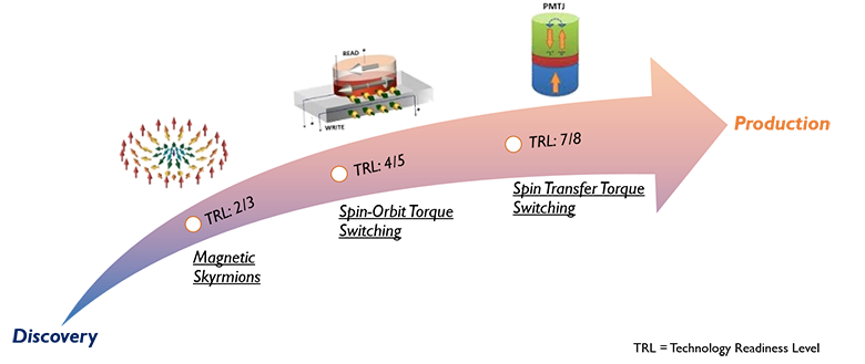
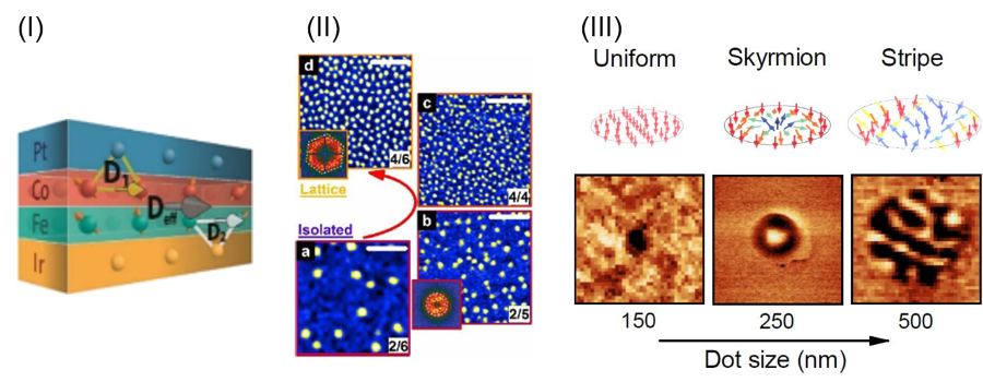
Figures adapted from A. Soumyanarayanan et al., Nature 539, 509-517(2016).

The emergence of connected electronic devices with sensing and computing capabilities has ushered in the Internet of Things (IoT) era: the need for real-time decision making at the data source, or “edge intelligence”, has assumed increased significance. There is a growing need for developing high-performance computing hardware platforms with energy-efficient, GHz switching memory. Furthermore, the limitation of Moore’s law is being reached within conventional materials and present technologies. Thus, the quest to develop integrated, beyond-CMOS infocomm technology (ICT) platforms has also become increasingly important.

Next-gen ICT elements should 1) operate on an inherently shorter time scale enabling faster processing, 2) possess intrinsic stability and robustness for scalability, and 3) integrate seamlessly with conventional CMOS processes. While battery-powered edge devices would require non-volatile memory (NVM) platforms for scaling up such capabilities, emerging NVM solutions are read-optimised — inherently limited in high-performance switching characteristics required for these applications. Bridging this large performance gap first requires moving towards NVM technology platforms whose “normally-off” state can drastically reduce power consumption.

The field of spintronics is focused on exploiting electron spin as a degree of freedom for applications in solid-state devices. Earlier pioneering works successfully exploiting both giant magnetoresistance (GMR) and tunnelling magnetoresistance (TMR) effects and formed the basis of reading and memory storage applications in electronic devices today, through the use of GMR read heads in hard disk drives for storage and magnetic tunnelling junctions (MTJ).

Next generation spintronics technologies are sought to create devices with lower switching power, faster dynamics and higher endurance. One such avenue is via spin transfer torque (STT) — currently in manufacturing — where a spin polarised current can be used to control the magnetisation of a magnetic layer.

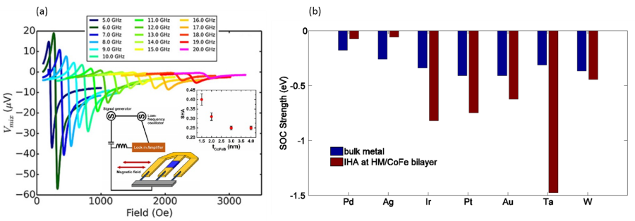
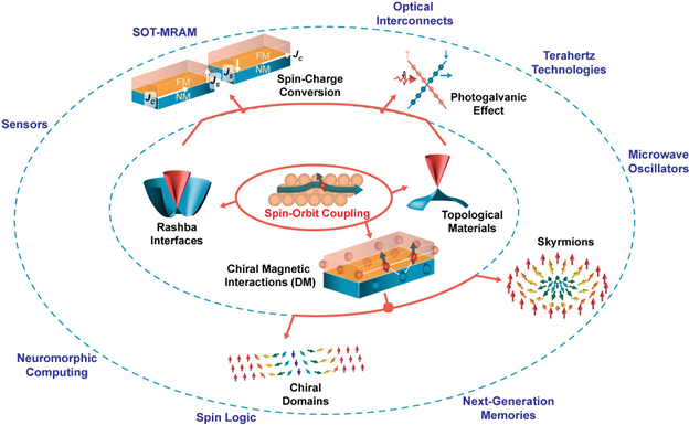
One particularly attractive avenue is the coupling of electron spin and momentum, known as spin-orbit coupling (SOC), recently found to be greatly enhanced at heavy metal (HM) – ferromagnet (FM) interfaces. Such interfaces are commonly used within existing MRAM stacks for incidental purposes. Interfacial SOC provides a fast, energy-efficient means to switch magnetisation, and creates new topological phases (topological materials, skyrmions etc.) that are robust at room temperature (RT). The practical utility of these recently discovered phenomena is imminent given the inherent CMOS compatibility of host materials.

Spin Transfer Torque

Over the years our team has developed in-depth understanding of spin-transfer torque (STT) switching and proposed novel solutions to improve memory devices performance in particular from the materials and stack design perspectives. STT writing involves applying currents through an oxide barrier of a magnetic tunnel junction (MTJ). The MTJ resistance is determined by the relative magnetisation directions of FL (free layer) and RL (reference layer). The distinct resistance of the two existing states (AP/ P) correspond to storing a binary ‘1’ or ‘0', respectively. The switching process is affected by various factors, such as the current density, the temperature, and the MTJ size, material selections, and process damages etc.1-5 Interestingly, the switching speed is less temperature-dependent in the precessional regime and become highly temperature-dependent in the thermal activation regime1.

One of our recent experimental studies showed non-collinear structure can deliver ∼53% reduction in critical current density in STT switching without compromising on the thermal stability of the devices. This advantage in switching current performance using the non-collinear stack was found to sustain down to ∼20 nm MTJs1

2020 11 23 SpEED 3
Figure from Ref [1]. Size dependence of various MTJs against the parameters of (a)TMR (b) switching current (c) thermal stability, and (d) efficiency. The blue colored symbols are for a non-collinear MTJ stack compared against a standard MTJ stack (orange).

Electric Field Assisted Switching

We also explore alternative low power writing schemes in MTJs is by means of voltage-controlled magnetic anisotropy. We demonstrated that electric field (EF) devices can be switched at a record speed of approximately 0.6 ns with write energies as low as 7 fJ. We did a comprehensive study on the role of the free layer thickness in electric-field controlled nanoscale perpendicular MTJs2. The development of EF-controlled MRAM will be relied upon optimisation of voltage-controlled magnetic anisotropy (ξ) and voltage modulation of coercivity (Hc). Numerous simulation and modelling works have been done, for example, we investigated the possibility of enhancement of voltage-controlled magnetic anisotropy by inserting of an oxide monolayer3.

Prototyping

We have also assimilated substantial experience in sub-100 nm MTJ fabrication and process integration with in-house development of a 1Mb STT-MRAM CMOS chip, and thereby established a detailed understanding of variations arising from the fabrication process. To further mitigate memory read and write errors, we have invested extensive efforts on designing error correction codes (ECCs) for NVM in recent years. 

Key Contacts

Dr. Lim Sze Ter, Lim_Sze_Ter@imre.a-star.edu.sg
Dr. James Lourembam, james_lourembam@imre.a-star.edu.sg

Spin Orbit Torque

Spin-orbit torque (SOT) is promising for GHz low-power switching of MTJs with high endurance towards integrated low-power computing because of its attractive non-volatile solutions to currently existing power-hungry volatile cache memory technology (static RAM). Realisation of field-free SOT is the most important challenge towards its practical application. Our works towards various schemes for field-free SOT switching, which have scalability and higher performance promise, involve materials studies, device design and characterisation, materials device simulations and CMOS integration.

We are also exploring the fundamental physics of SOT phenomena and optimisation studies. For example, it is important to study and enhance the charge-to-spin conversion efficiency. We use spin-torque ferromagnetic resonance (ST-FMR) to quantify the spin Hall angle and the damping parameters. In particular, enhanced SOT efficiency may be achieved by engineering FM-based heterostructures and interfaces. We recently demonstrated that substantially large effective spin Hall angle can be achieved with proper stack materials selection, one such example is the Ta/ CoFeB/ Pt stack1. In another study, we investigate the spin-orbit interaction in HM/ CoFe bilayers using first-principles calculations2. Charge transfer at the HM/ CoFe interface results in an interfacial electric field, as well as spin and orbit moments at the interfacial heavy atom. Spin-orbit coupling (SOC) with various materials was studied by comparing the SOC strength at the interfacial heavy atom (IHA) with its bulk value at corresponding transition metal. Our work suggests that interfacial electric field plays an essential role in tuning the SOC effect at HM/ CoFe bilayers, which might be exploited for magnetic switching of SOT-based spin-orbitronic devices.

2020 11 23 SpEED 4(resized)
(a) Figure from Ref [1,2]  Typical ST-FMR setup along with its spectra; (b) First principles calculation of SOC strength. The brown bars display the SOC strength of IHA at the HM/ CoFe bilayer. The blue bars represent the SOC strength of heavy elements in its bulk.
In addition, our team recently revealed that the existence of interfacial Dzyaloshinskii-Moriya interaction at the HM/ FM interface can induce field-free spin-orbit torque switching of perpendicular magnetisation3. This can be incorporated using a heterostructure free layer (DMI at the interface of FM and SOT channel) to induce switching without sacrificing the free-layer magnetic anisotropy. We discover a regime for deterministic switching against current and DMI variations. This work is directly relevant for field-free SOT by tuning DMI strength through materials engineering. 
2020 11 23 SpEED 5(resized)
(c) Schematic of a 3-Terminal SOT device; (d) The sign of DMI may impose boundary conditions at the edge of the MTJs; (e) Dynamics of perpendicular magnetization component, Mz under various D and Hx (in-plane field) conditions (pulse is applied within the shaded region). The dashed curve indicates magnetisation switching is observed without the presence of magnetic field if DMI is introduced.

Key Contacts

Dr. Lim Sze Ter, Lim_Sze_Ter@imre.a-star.edu.sg
Dr. James Lourembam, james_lourembam@imre.a-star.edu.sg

Skyrmions

2020 11 23 SpEED 6(resized)
(I) Schematic of Ir/Fe/Co/Pt multilayer stack. The large DMI vectors at Co/Pt (D1) and Fe/Ir (D2) interfaces act in concert to enhance the effective DMI, Deff. (II) By varying the Fe/Co thicknesses, the magnetic interactions in the multilayer stack can be continuously modulated, enabling a platform for tunable skyrmion size, density, and configuration at room temperature. (III) Zero field skyrmions stabilised at intermediate dot sizes, with uniform magnetisation and labyrinth stripe phases for smaller and larger dot sizes, respectively.

Magnetic skyrmions are nanoscale spin structures with topological properties that have been recently discovered in several material systems. Due to their topologically protected spin structure, skyrmions behave like finite-sized magnetic particles that can be (a) packed into dense nanoscale arrays, (b) singly created, switched, and deleted, and (c) moved controllably at low current densities. Skyrmions are thus natural candidates for next-generation memory: forming high-density cells with potential fast switching and low power readout. The discovery of room temperature (RT) skyrmions in technologically relevant sputtered multilayer films triggered an explosion of efforts to modulate their physical properties towards fast-tracking the imminent realisation of skyrmion-based technologies. Acquiring deterministic control over skyrmion formation and properties requires the ability to tailor the parent magnetic interactions. Skyrmions are formed in multilayer thin films due to the presence of the chiral Dzyaloshinskii-Moriya interaction (DMI) at ferromagnet (FM) – heavy metal (HM) interfaces.

Skyrmionic Materials

One of our signature achievements is the world-first realisation of tunable room temperature (RT) skyrmions in multilayer thin film systems. We can tune the magnetic interactions in the system by varying the relative composition of iron and cobalt, leading to corresponding variation of the skyrmions’ sizes and configurations, as shown in Fig. (i). These RT skyrmions have been detected and characterised by three complementary magnetic microscopy techniques (MFM, MTXM, and L-TEM), providing an established recipe for quantitative imaging of single skyrmions in device configurations. Importantly, demonstrable electrical detection of these skyrmions via Hall transport has immediate relevance for device applications.

Skyrmionic Devices

We have also demonstrated confinement-induced skyrmion formation and evolution at zero magnetic field in dot structures fabricated from these multilayers. As seen in Fig. (ii), by tuning the dot width and relative composition of iron and cobalt, sub-100nm skyrmions were observed to be stabilised at zero field. This first realisation at such a small scale makes it immediately applicable in current technological lines especially within MTJ devices, as well as future applications such as microwave detectors, oscillators, and multi-bit devices.

Key Contacts

Dr. Anjan Soumyanarayanan, anjan@imre.a-star.edu.sg
Dr. Ho Pin, ho_pin@imre.a-star.edu.sg


Capabilities

2020 11 23 SpEED 7(resized)
The SpEED program has well-established capabilities for achieving its scientific and technological objectives. The effort strategically integrates capabilities in the areas of 1) Materials and Device Development, 2) Microscopy and Modelling, 3) Electrical Transport Measurements, and 4) 200 mm wafer-level scaling. The fabrication and translational components utilise a well-established 200 mm semiconductor fabrication platform which has been successfully used for multiple industry collaborations. The programme provides many pathways for near-term engagement with local foundries and chip manufacturers, and long-term capabilities for sustained value capture in the burgeoning field of edge computing.


Materials & Device Development

(a) Film Deposition

  • Custom-designed Chiron™ PVD system consisting of 8 DC and 2 RF targets, with built-in in-situ atomic layer deposition system, for film deposition on 100 mm wafers and coupons with sub-angstrom precision.

(b) Film Characterisation

  • Magnetic analysis using vibrating sample magnetometer (VSM Model EZ11), alternating gradient magnetometer (MicroMag Model 2900) and superconducting quantum interference device (SQUID MPMS). 
  • Structural/electronic/chemical analysis using x-ray diffraction (Bruker™ 2D Micro, PANalytical X’Pert™), x-ray reflectivity, x-ray photoelectron spectrometry (Theta Probe XPS) and ellipsometry.
  • Electrical analysis using Capres current-in-plane tunneling tool to determine film level tunnelling magnetoresistance and resistance-area with magnetic fields up to 0.6 T.
  • Imaging analysis using atomic force and magnetic force microscopy, transmission electron microscopy, scanning electron microscopy elaborated in the following section.

(c) Device Fabrication

  • Lithography tools such as EVG™ mask aligner and Elionix™ electron beam lithography (EBL) system with ~1.5 μm and ~10 nm resolution, respectively.
  • Reactive ion etch (IntlVac™) for milling. 
  • Thermal/electron beam evaporators (EvoVac™) for metallisation.

Microscopy & Modelling

  • Atomic force and magnetic force microscopy (DI 3100 SPM & Bruker ICON™) capable of producing non-perturbative, high contrast and spatial resolution images.
  • Transmission electron microscopy (JEOL 2100 TEM/Philips CM300 FEGTEM) giving high resolution cross-sectional images for determining spacer roughness, stack thickness, cell profile, as well as elemental mapping of individual layers using energy dispersive x-ray analysis and electron energy loss spectroscopy. The FEI Titan™ is also equipped with Lorentz and holography capabilities for analysing magnetic textures at variable fields and temperatures.
  • Magnetic transmission x-ray microscopy at the XM1 beamline in Lawrence Berkeley National Laboratory, USA, with full field transmission x-ray magnetic circular dichroism contrast, for imaging magnetic textures with ~30 nm resolution deposited on thin membranes.
  • Device and circuit design modelling (e.g. MuMaX3, OOMMF, VASO, SPICE) leveraging on Petascale supercomputing facilities at the National Supercomputing Centre (NSCC).

Electrical Transport Measurements

  • Custom-made electrical device testing platforms and probe stations with pulsing capabilities <1 ns and noise levels down to ~1nV.
  • Cryostats and physical property measurement system for low temperature magneto-transport measurements (2 K, 9 T).
  • ISI Wafer auto-prober capable of conducting device testing modules including TMR, switching voltage, endurance, write error rate, read error rate, breakdown voltage.
  • Custom-made high-resolution broadband and spin-torque ferromagnetic resonance systems with frequency range of 67 GHz in magnetic fields up to 1 T and variable temperature operation. 

200 mm Wafer-Level Scaling

(a) Device Stack Deposition Tool 

  • Singulus Timaris cluster sputtering system with pre-cleaning, annealing, wedge deposition and multi-target (over 20) process modules at 2 Å thickness uniformity.

(b) Copper Protocol Fabrication Line

  • Spin coating & developing using Silicon Valley Group SVG 90S
  • Lithography using Canon EX5 248 nm DUV Stepper
  • Hard mask etch using advanced dielectric etcher (SPTS Etch system) or induced coupled plasma (ICP)-fluorine based chemistry etching (Oxford PlasmaPro System 100 cobra ICP)
  • Cell etch using Oxford Ionfab 300Plus (Ion milling)
  • Cell passivation and insulation using OIPT Plasmalab System 380
  • Descum using Axcelis Ashing System
  • Chemical mechanical polishing using Okamoto SPP600S
  • Electrode deposition using Singulus Rotaris Cluster System or AMAT Endura System
  • Annealing using horizontal annealing furnace

(c) Prototyping

  • Simulation packages including industry standard Verilog-A, electronic design automation (EDA) and computer aided drafting (CAD) for the design of a viable integrated circuit consisting of a microscopic electronic circuit array of SOT-based devices.
  • Simulated IC designs implemented on testing platform such as field programmable gate arrays (FPGA) and printed circuit boards (PCB) and tested on high speed and precision analogue/digital characterisation circuits and device specific read/write circuits.


Achievements

Selected Publications and IPs

Spin Transfer Torque

  1. J. Lourembam et al.,“A non-collinear double MgO based perpendicular magnetic tunnel junction”, Appl. Phys. Lett. 113, 022403 (2018)
  2.  J. Lourembam et al.,“Role of CoFeB thickness in electric field controlled sub-100 nm sized magnetic tunnel junctions”, AIP Advances, 8, 055915 (2018)
  3. M. Zeng et al.,“Large electric field modulation of magnetic anisotropy in MgO/CoFe/Ta structures with monolayer oxide insertion“, Appl. Phys. Lett. 113, 192404 (2018)
  4. J. Lourembam et al., “Thickness-Dependent Perpendicular Magnetic Anisotropy and Gilbert Damping in Hf/Co20Fe60B20/MgO Heterostructures” ,Phys. Rev. Appl. 10, 044057 (2018)
  5. A. Okada et al. ”Magnetization dynamics and its scattering mechanism in thin CoFeB films with interfacial anisotropy”,  PNAS 114, 3815 (2017)
  6. Magnetoelectric device, method for forming a magnetoelectric device, and writing method for a magnetoelectric device. (US patent:US9601174B2)
  7. Magnetoresistive device and a writing method for a magnetoresistive device. (US patent: US9058885B2)
  8. Methods and circuit arrangements for determining resistances. (US patent: US9697894B2)
  9. Memory device with soft-decision decoding. (US patent: US8917540B2)

Spin Orbit Torque

  1.  L. Huang et al.,“Engineering magnetic heterostructures to obtain large spin Hall efficiency for spin-orbit torque devices”, Appl. Phys. Lett. 113, 022402 (2018)
  2. M. Zeng et al.,“Interfacial electric field and spin-orbitronic properties of heavy-metal/CoFe bilayers”, Appl. Phys. Lett. 114, 012401 (2019)
  3. B. Chen et al.,“Field-free spin-orbit torque switching of a perpendicular ferromagnet with Dzyaloshinskii-Moriya interaction”, Appl. Phys. Lett. 114, 022401 (2019)

Skyrmions

  1. A.Soumyanarayanan et al., “Emergent phenomena induced by spin–orbit coupling at surfaces and interfaces”, Nature 539, 509–517 (2016).
  2. A.Soumyanarayanan et al., “Tunable room-temperature magnetic skyrmions in Ir/Fe/Co/Pt multilayers”, Nature Materials 16, 898-904 (2017).
  3. A.Yagil et al., “Stray field signatures of Néel textured skyrmions in Ir/Fe/Co/Pt multilayer films”,  Appl. Phys. Lett. 112, 192403 (2018).
  4. P. Ho et al., Geometrically Tailored Skyrmions at Zero Magnetic Field in Multilayered Nanostructures”,  Phys. Rev. Applied 11, 024064 (2019).
  5. M. Raju, A. Yagil et al., “The evolution of skyrmions in Ir/Fe/Co/Pt multilayers and their topological Hall signature”, Nature Communications 10, 696 (2019).

Publicity and Media Coverage

1. EE Times
2. A*STAR Research
3. Young Scientist Awards 2018
4. Asian Scientist Magazine

Contact