Introduction
Wide bandgap semiconductors are essential for the next generation high-efficient power and radio-frequency electronics, with their key deployment envisaged for large scale applications in power conversion, communications, and lightings. Recent technological trends show the dominance of SiC and GaN based materials systems offering higher breakdown voltage, lightweight, and fast switching response. The main issues in such semiconductors are associated with the presence of defects in the large diameter bulk substrates and epitaxial wafers. Our research and development efforts are focused on the growth and characterization of such semiconductor materials, and to reduce the defect density in SiC and GaN epitaxial wafers toward manufacturing adoption on 150 and 200 mm diameter platforms.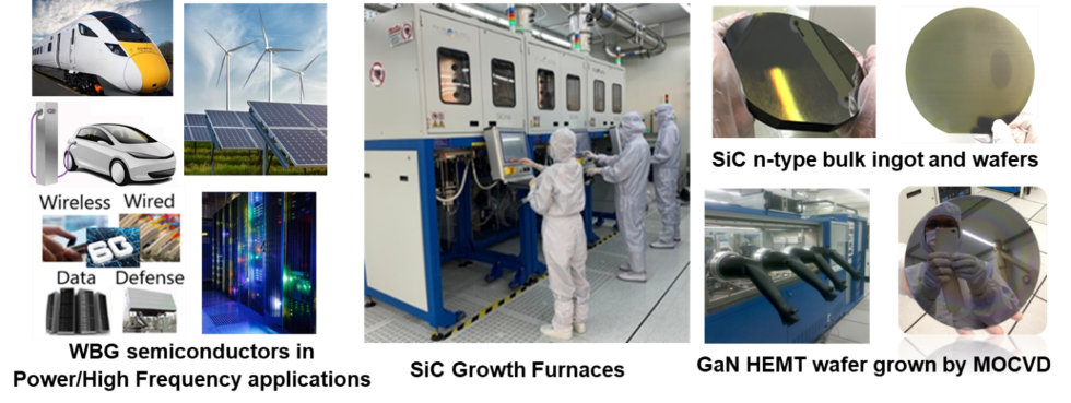
Capabilities
Our dedicated team has plenty of research experience in compound semiconductor materials and their processing. The research group has been developing expertise and capabilities in the following wide bandgap semiconductor platforms:
- MOCVD growth of GaN: Up to 200 mm diameter epitaxial growth with wafer level characterization, defect analyses, in-situ SiN passivation, buffer structure optimization, in-situ multi-wavelengths reflectance and curvature profiling, wafer bow control with structural and electrical homogeneity in epitaxial wafers on silicon, sapphire and silicon carbide substrates.
- Bulk and Epitaxial growth of SiC: 4H-SiC bulk growth with understanding of defect formation and reduction during 150 to 200 mm physical vapor transport (PVT) processes, high-temperature hotwall CVD for 4H-SiC homo-epitaxial growth with thickness suitable for 1.0 kV to >10 kV application potentials.
- Characterization of wide bandgap semiconductor materials: 200 mm wafer level HRXRD for rocking curves, reciprocal space mapping (RSM), X-ray reflectivity (XRR), Optical spectroscopy using UV-Vis micro PL and micro-Raman scattering, SiC epilayer thickness mapping, Electrical characterization of GaN and SiC epitaxial wafers with breakdown voltage measurements.
Achievements
- Epitaxy solutions for GaN-on-Silicon high voltage electronics: Use of AlN and multiple intermediate layers to reduce the crack and defect density in 200 mm HEMT stack process tuning, with high buffer breakdown structures up to 1000 V and 650 V HEMTs with gate leakage current <nA/mm, Demonstrated Au-free HEMTs with ON-OFF ratio >109 and with lower channel temperatures.
- Unique AlN epitaxy to reduce Al/Ga diffusion and reduced auto-doping at the AlN/HR-Si for RF HEMTs, with demonstration of GaN-on-Si transistor wafers for fmax >100 GHz high frequency operation.
- Materials development using AlGaN/GaN and InAlN/GaN HEMT stacks as UV detector structures on Si exhibiting ultra-high responsivity, GaN-based chemical sensing and micro-mechanical systems.
- Development of SiC ingots and substrates using modified PVT processes for 150 and 200 mm wafering, design of graphite hot-zones with customized crucibles and insulator assembly for 4H-SiC bulk growth, establishment of a supply chain system from SiC source raw materials up to preparation of epiready substrates by dicing/grinding/polishing, established materials characterization protocols for SiC defect identification, and isolation on both bulk SiC substrates and epitaxial 4H-SiC layers.