Research Focus
The control and manipulation of physical objects at the quantum level have progressed considerably in the past decade. This quantum control promises fascinating advances in both technology and fundamental science. For example, use of quantum phenomena in data systems allows one to speed up computation and database search algorithms as well as development of highly secure communication networks. The same physical principles also lead to the development of a new family of highly sensitive optical and solid-state based sensors with highest resolution. However, translation from proof-of-concept laboratory demonstrations of quantum devices to practical applications is quite immature. In our group we exploit new technologies to make quantum tools accessible beyond the laboratory. We develop prototypes of quantum networks and coherent interconnects for manipulation of quantum information. We are also actively working on optical quantum sensors for environmental monitoring and material analysis.
In addition we are exploring applications of quantum techniques across multiple disciplines, including nano-photonics and biology. The unique control over quantum systems enables us to develop new generations of sensors and grasp the finest details of biological processes.
For a list of our recent Highlights and Publications, click here.
Research Topics
a) Integrated quantum photonics
Quantum information networks are at the forefront of practical applications of quantum technology. Quantum networks employ stationary quantum systems as nodes which process and store quantum information. The nodes are connected by quantum links, which transfer quantum information from one node to another.
Two of the biggest challenges for large-scale quantum networks are (1) Efficient connection between stationary nodes and their optical links, which provides high-fidelity transmission and (2) A scalable and fabrication-friendly platform, which accommodates both stationary nodes and their optical links. Any platform built to overcome these challenges need to satisfy compatibility requirements for different materials, operation wavelengths, and temperatures.
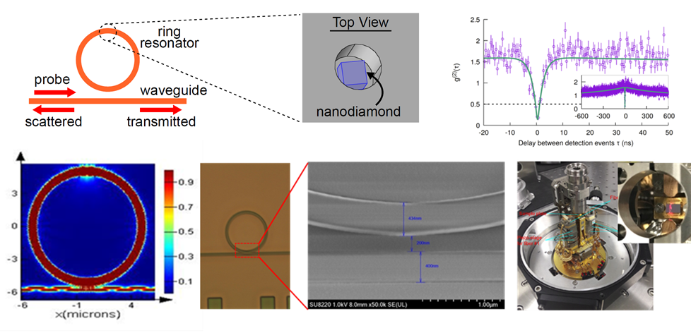
Our objective is to push the practical implementation of quantum networks by using integrated photonic technologies. We encode quantum information in spin states of atomic defects in diamond nano-particles and use them as stationary nodes. Nanodiamonds are interconnected via optical waveguides made of low-loss Silicon Nitride. Optically-resonant nanostructures enhance the coupling of photons emitted from the nano-diamonds into waveguides [optics comm 2017]. Photons interfere on the same optical chip and create quantum entanglement between different nodes. This allows execution of quantum networking protocols and quantum logic on the same optical chip. For readout of quantum information, we develop on-chip single photon sensitive photodetectors (SPADs). This scalable and intrinsically stable platform will allow us to generate, transfer, manipulate and detect quantum information [Optics Express 2018, IEEE 2019, Arxiv 2020].
The physics concepts, developed for quantum information can be applied to applications in magnetometry at room temperature. We use integrated optics to improve the sensitivity of diamond-based magnetometers. The technology will lead to the development of a new family of highly sensitive electromagnetic field sensors with nanometer spatial resolution [PRB 2016].
b) Infrared metrology with visible light
Infrared (IR) measurements provide unique information about materials, which is useful for many applications. Current implementations of IR-metrology require using specialized light sources, optical components, and detectors suitable for the operation in the IR range. These components often have inferior performance and they are more costly in comparison to their visible range counterparts.
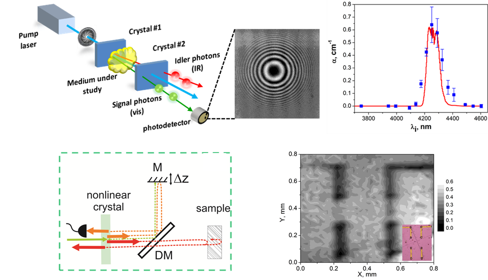
In this project, we develop a practical alternatives to existing IR systems which allow us to carry measurements of absorption, refraction and imaging in the IR range using visible range optics [Nature Photonics 2016, Scientific reports 2017, Light: Science and Applications 2020]. The concept is based on the interference of entangled photons obtained via spontaneous parametric down conversion (SPDC). In our interferometer, conventional mirrors are substituted by nonlinear crystals, where the SPDC occurs. Down-converted photons (signal and idler) from the first crystal interfere with those from the second crystal. The interference for signal photons depends on amplitudes and phases of all the three interacting photons: the pump (visible range), the signal (visible range), and the idler (IR range). Therefore, the properties of idler photons in the IR range can be inferred from the signal photon in the visible range. Detection of IR photons is not needed.
In our experiments, we study IR absorption spectrum of carbon dioxide (CO2) gas, polymer samples, and silicon wafers [NJP 2017, APL 2020]. We were able to measure the absorption coefficient and the refractive index of samples in a broad spectral range with high resolution. We also realized the concept of IR optical coherence tomography with visible light [Quantum S&T 2017] and the wide-field hyperspectral imaging [Science Advances 2020]. The developed techniques can substitute and/or complement conventional methods techniques, as they use well-developed components for the visible range.
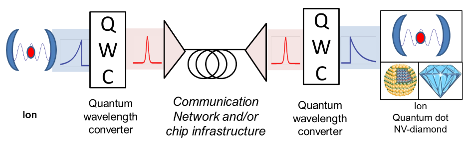
c) Frequency conversion of single photons for quantum networking
Great interest in quantum information science is focused on theoretical and experimental studies of quantum information networks. These networks employ stationary quantum systems as nodes which process and store quantum information. The nodes are connected by quantum links, which transfer quantum information from one node to another. Deployment of quantum networks allows to scale-up and to accelerate processing and distribution of quantum information. Implementation of quantum networks will have a revolutionary impact on the way we manipulate and transmit the data.
Trapped ion technology is one of the most promising platforms for the realization of stationary nodes in quantum networks. Trapped ions have comparatively long coherence times, during which, it is feasible to record, manipulate and read-out quantum information with high fidelity. Optical links between the ions are used for transfer of quantum information. Impressive progress has been achieved on reducing the footprint of ion traps and on increasing the number of optical interconnections between ions.
One of the biggest challenges in the realization of large-scale quantum networks with trapped ions is the mismatch between wavelengths of ion emission (typically in near-UV) and the transmission window of conventional optical fibers (in near-IR). In this project we aim to develop a new class of optical devices for coherent wavelength conversion of single photons emitted by trapped ions. The approach is based on the use of the high index and highly nonlinear materials that are transparent in the wavelengths emitted by trapped ions. We design novel nanophotonic structures which can provide low loss, high conversion efficiency, broadband operation and on-chip integration [Nanoletters 2020].