Semiconductor R&D and Innovation at A*STAR, Singapore
More powerful computing, faster connectivity and more efficient energy use all depend on advances in semiconductor technology.

The A*STAR-hosted Research, Innovation and Enterprise (RIE) Flagship in Semiconductors will set national R&D roadmaps and strengthen our existing capabilities. A*STAR supports this through expertise in radio frequency gallium nitride (RF GaN), piezoelectric micro-electro-mechanical systems (PiezoMEMS), silicon photonics, flat optics, advanced packaging, power electronics and integrated circuit design.
To translate these strengths into industry applications, A*STAR connects research expertise, shared industry-grade facilities and industry partnerships through initiatives led by the A*STAR Institute of Microelectronics (IME) and supported by the National Semiconductor Translation and Innovation Centre (NSTIC). Beyond its R&D platforms, A*STAR and the Singapore Economic Development Board (EDB) jointly drive SG Semiconductor, uniting Singapore’s semiconductor ecosystem under a shared national identity. These concerted efforts help companies accelerate innovation from lab to fab for long-term industrial and economic impact.
Singapore produces about one in ten chips and one-fifth of semiconductor manufacturing equipment worldwide. With global industry revenue expected to grow by US$300 billion over the next five years, driven in large part by AI, Singapore is well positioned to contribute to this growth. Its manufacturing base sits alongside research institutions, universities and technology partners, connecting basic research with process development and manufacturing expertise. SG Semiconductor brings this connected ecosystem together under a shared national identity, providing one-stop access to Singapore’s semiconductor ecosystem.
As part of the RIE 2030 Plan, Singapore is investing an additional S$800 million to strengthen national semiconductor R&D platforms for companies to co-develop and translate next-generation technologies.
8,000 square metres of cleanroom facilities equipped with industry-grade semiconductor R&D tools, with a new 12-inch fab at JTC nanoSpace @ Tampines adding a further 9,000 square metres from 2027.
A*STAR offers companies a multidisciplinary route from semiconductor research to industry translation. Decades of sustained investment have built deep engineering capabilities and key national platforms that position Singapore as a key node in the global semiconductor supply chain.
A*STAR addresses complex semiconductor challenges and translates cross-disciplinary research into industry-relevant solutions.
A*STAR brings together specialised semiconductor capabilities spanning advanced packaging, photonics, MEMS, power electronics, RF technologies and integrated circuit design.
A*STAR extends its semiconductor expertise in materials, photonics and device fabrication to next-generation quantum hardware. This effort supports the National Quantum Strategy driven by the National Quantum Office (NQO).
National-level quantum programmes, such as the A*STAR-hosted National Quantum Federated Foundry (NQFF), provide the best combined capabilities in quantum device design, fabrication and characterisation in Singapore, alongside research and innovation activities at A*STAR’s Institute of Microelectronics (IME) and Institute of Materials Research and Engineering (IMRE).
As part of SG Semiconductor, we work closely with industry partners, aligning research with real-world needs to provide a clear path from promising research to validated, deployable technologies.
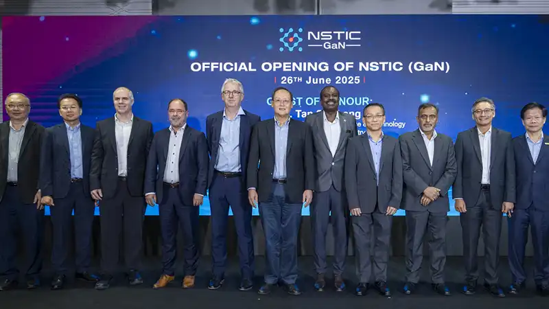
A*STAR works with industry partners from prototyping and manufacturing through to commercial scaling. NSTIC (GaN) enables factory-floor prototyping and validation, attracting more than ten partnerships with companies including Incize and Rohde & Schwarz.
The Lab-in-Fab joint laboratory with STMicroelectronics and ULVAC helps companies scale PiezoMEMS innovations to volume production without process recreation and revalidation.
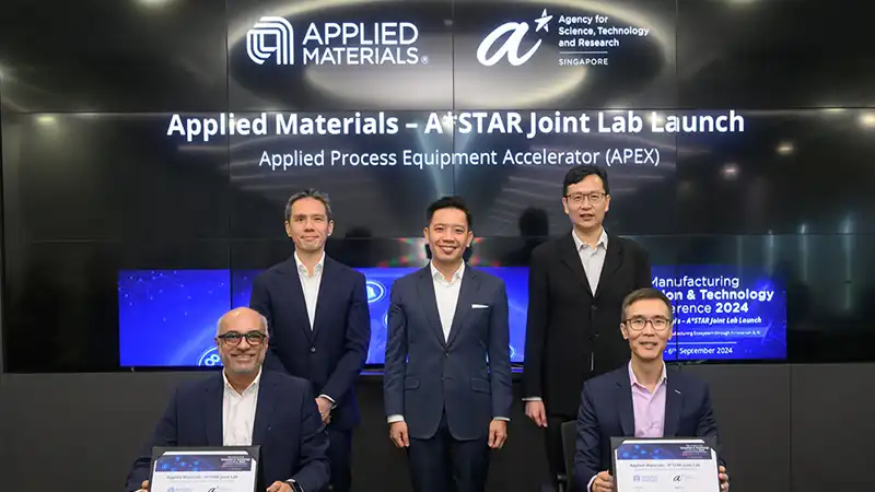
A*STAR’s longstanding partnership with Applied Materials through the Centre of Excellence in Advanced Packaging has strengthened Singapore’s position in advanced packaging R&D. Since the third phase of the Joint Lab was established in 2021, more than 30 projects involving 50 companies have been initiated, 300 individuals trained and more than 40 SMEs involved.
A*STAR’s silicon photonics programme gave rise to Advanced Micro Foundry, which GlobalFoundries acquired in 2025, while NSTIC (Advanced Photonics) continues to advance national capabilities. Building on collaborations spanning PiezoMEMS, advanced packaging and silicon photonics, A*STAR and GlobalFoundries continue to advance silicon photonics technologies and expand R&D capabilities in Singapore.
A*STAR and MetaOptics Technologies co-developed rapid-prototyping technology and metalenses for mass production, contributing to the commercialisation of new products and the company’s subsequent SGX Catalist listing.
Do your boldest and most impactful work with A*STAR. Tackle industry-relevant semiconductor challenges with access to advanced R&D platforms and facilities, and opportunities to collaborate across the semiconductor ecosystem.
Discover how A*STAR scientists and researchers are shaping Singapore’s semiconductor future.
Explore semiconductor jobs, scholarships, internships and research attachment opportunities at A*STAR.
Explore research and technical roles available across A*STAR and contribute to Singapore’s semiconductor research and innovation ecosystem.
Pursue graduate research and develop expertise in semiconductor science and technology through A*STAR’s scholarship programmes.
Gain hands-on research experience through internship opportunities for PhD, Masters, undergraduate, JC and polytechnic students.
Undertake research attachments at A*STAR and work alongside researchers advancing science and technology in Singapore.

Collaborate with A*STAR to accelerate next-generation Semiconductor technologies.
A*STAR supports semiconductor R&D translation across advanced packaging, advanced photonics, silicon photonics, power electronics, RF GaN, silicon carbide, flat optics, piezoMEMS and integrated circuit design. Through A*STAR IME, IMRE and NSTIC, A*STAR helps companies move from research validation towards industry deployment and manufacturing readiness.
SG Semiconductor is the national identity for Singapore's semiconductor ecosystem. It brings together semiconductor companies, research institutions, universities and government agencies around a shared ambition to strengthen Singapore's position as a globally competitive hub for semiconductor innovation, manufacturing and talent.
As Singapore's lead public sector R&D agency, A*STAR helps drive SG Semiconductor together with EDB by connecting research, industry and talent. Working alongside companies, universities and ecosystem partners, A*STAR develops strategic semiconductor capabilities, operates shared R&D infrastructure, nurtures talent and supports the translation of emerging technologies into manufacturing-ready solutions. These efforts strengthen Singapore's competitiveness across the global semiconductor value chain.
A*STAR’s core semiconductor focus areas are advanced packaging and advanced photonics. These are supported by complementary capabilities in flat optics, piezoMEMS, RF and cryogenic IC design, RF GaN and SiC technologies.
A*STAR IME supports advanced packaging R&D for applications such as AI, 5G, automotive systems and hyperscale data centres. Its capabilities include heterogeneous chiplet integration, system-in-package solutions, fan-out wafer-level packaging, 2.5D interposers, 3D TSV and hybrid bonding.
A*STAR develops advanced photonics technologies for faster, more energy-efficient data movement and scalable optical interconnects. Its photonics capabilities include silicon photonics, silicon nitride photonics, heterogeneous photonics integration, flat optics and sensor platforms.
The National Semiconductor Translation and Innovation Centre, or NSTIC, enables semiconductor translation by connecting research capabilities, industry partners and shared infrastructure.
A*STAR’s NSTIC R&D Fab will provide 12-inch industry-grade tools and shared cleanroom access at JTC nanoSpace @ Tampines from 2027. It is intended to help companies scale semiconductor innovations from lab to fab, especially in areas such as advanced packaging translation.
Companies can collaborate with A*STAR through industry partnerships, co-development projects, licensing and access to A*STAR’s research talent, facilities and technology platforms. A*STAR’s Innovation & Enterprise group supports companies in moving research from lab to market through partnerships, commercialisation and venture building.
A*STAR supports IP commercialisation through co-development and licensing arrangements. Its Innovation & Enterprise group works with businesses and partners to translate research and intellectual property into market-ready products and services.
Startups and SMEs can work with A*STAR to access research expertise, co-development pathways and capability-building programmes. For local SMEs, A*STAR’s T-Up programme seconds A*STAR scientists and research engineers to companies for R&D projects, while EDA Garage supports local semiconductor companies with more accessible chip design tools and training.
Yes. A*STAR works with both local and global businesses, including MNCs, local enterprises and startups. Partnership scope depends on the project, programme eligibility and alignment with Singapore’s semiconductor R&D and innovation ecosystem.
A*STAR’s semiconductor work supports Singapore’s RIE2030 priorities by strengthening national capabilities in advanced packaging, advanced photonics and semiconductor translation. MTI announced an S$800 million RIE Flagship in Semiconductors focused on high-impact areas such as advanced packaging and advanced photonics.
A*STAR offers semiconductor R&D roles for professionals, as well as scholarships, internships and research attachments for students and early-career researchers. The semiconductor page highlights opportunities including the A*STAR Graduate Scholarship, IME internships, research internship awards, PhD training and research attachment programmes.
Meet A*STAR researchers and industry partners at semiconductor events such as Innovate Together, which features technology presentations, discussions and collaboration opportunities. Explore the event programme to find sessions relevant to your interests, or contact A*STAR to discuss a semiconductor R&D collaboration.