Using ScAlN-based pyroelectric detector, IME also developed a low-power contactless button sensing system in order to reduce disease transmission through touch. Our system requires ~3.5× lower power consumption compared to commercial contactless button.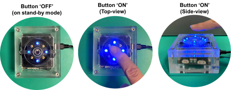 Presented at SPIE Photonics West 2023, Paper 12434-4. |
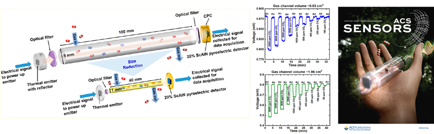
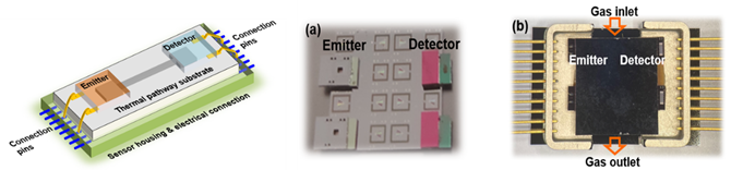
IME has demonstrated an on-chip CO2 gas sensor. This is constructed by integrating MEMS-based thermal emitter, ScAlN-based pyroelectric detector and a sensing channel. This integrated sensor has a small footprint of 13 mm x 13 mm. The integration of MEMS emitter, thermal pathway substrate, and pyroelectric detector, realized through CMOS compatible process, shows the potential for mass-deployment of gas sensors in environmental sensing networks.
Presented at SPIE Photonics West 2023, Paper 12426-29
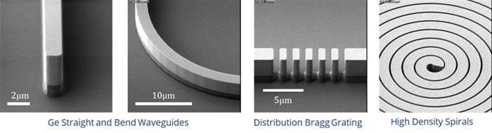
On-chip mid-infrared (MIR) spectrometer requires waveguide designs allowing small bending radius and meaningful interaction between the mode field and analyte. Germanium-on-Silicon (GOS) material system fits this requirement, yet their low index contrasts limit the bending radius to a few hundred micrometres range. IME has developed a unique high aspect ratio GOS waveguide with 3µm height and a gap spacing as small as 300nm. The minimum bend radius is decreased to 20µm. Various build blocks including in-plane distributed Bragg grating (DBR) structures, cascaded Fabry-Perot resonators, polarization splitters, and grating couplers are demonstrated
Leveraging on IME’s advanced 12-inch integration capability including the ArF immersion photolithography with minimum feature of less than 100 nm, we are able to develop low-loss SiN photonic integration platform with various SiN waveguide thickness over 12-inch wafers. With up to 800 nm SiN in thickness, the smallest critical dimension (CD) is less than 100nm for isolated line and 150 nm for dense structures with good uniformity. The minimum waveguide loss for single mode waveguide at O band is less than 0.5 dB/cm and 0.009 dB per 90o bend with 40μm in radius.
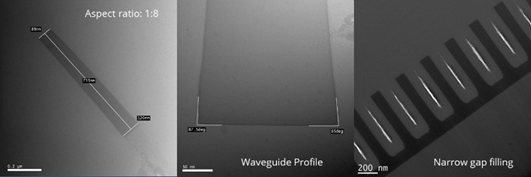
Additionally, ultra-low loss thin SiN waveguide platform is also developed and the quality factor of microring resonator is >10 million, with an extracted waveguide loss of as low as 0.04 dB/cm.
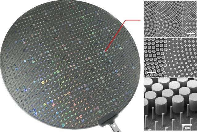
Flat optics make use of artificial nanostructured material, known as the metasurface. The metasurface consists of thousands of nanostructured scatterers that when subject to tailor-made design, are able to make full control of the electromagnetic properties including phase, amplitude and polarization. Metasurface manipulates the wavefront within an optically thin distance so that device miniaturization and integration are possible.
Leveraging on the superior optical flexibilities of flat optics, IME has demonstrated multiple key optical devices (metalens, wave-plate, meta hologram etc.) based on the nanostructured metasurfaces, covering a broad band wavelength range.
The patterning of sub-100nm nanopillars has been achieved by 193nm ArF immersion scanner on 12-inch wafers. Particularly, Si and SiN nanopillars with as high as 10 aspect ratio have been successfully demonstrated by inductive coupled plasma (ICP) etching.
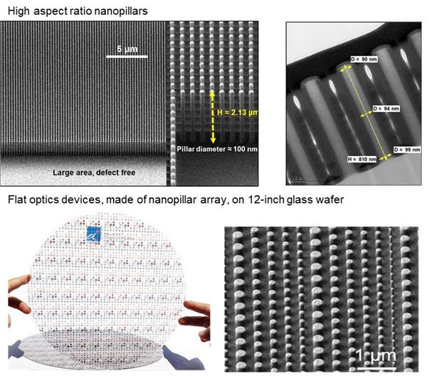
Mid-infrared (mid-IR) is a technologically important band crucial to many applications including thermal imaging, remote sensing and free-space communications. However, most of the mature materials are opaque in this range, making the development of mid-IR photonics challenging. To address this issue, IME demonstrated metalens devices fabricated on an 8-inch Ge-on-Si wafer for mid-IR regime. These demonstrated mass-producible metasurfaces can be potential solutions for next-generation mid-IR photonics.