System in package

IME's System in Package (SiP) group develops novel package architectures that serve a broad range of applications such as data centres, Mobile/5G, Internet of Things, Artificial Intelligence (AI), automotive and medical technology. These package designs are virtually modelled using sophisticated multiphysics simulation tools to determine their electrical, thermal, and mechanical behaviour. The advanced-package architecture is then brought to life through the use of IME's Advanced-Package-Design-Kit (APDK) and SiP design methodology. The package is manufactured in IME's state-of-the-art 300mm Advanced Packaging Development Line and is thoroughly tested, verified, and evaluated for reliability at IME's More-than-Moore Test Center. By utilizing the SiP platform at IME, our industry partners can prototype, sample, and produce advanced packages that are tailored to their specific end applications.

Advanced Intelligent Power Module (IPM) for EV/PHEV/HEV

As demand for EV/PHEV/HEV are on the rise, there are also the ever increasing demand for power modules with smaller form factor, higher power output, and higher operation temperature. Thus there is a need for the automotive industry to move from Silicon to Silicon Carbide, Si to SiC.
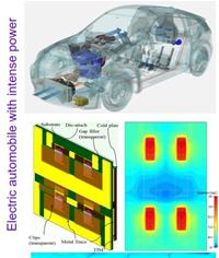
IME’s Advanced Intelligent Power Module (IPM) for EV/PHEV/HEV offers advance integrated double side liquid cooling and health monitoring solutions for the Inverter which converts DC from the vehicle’s batteries system to AC to drive it. Typically the inverter operates at high voltage and high current. IME technologies target to achieve 600W dissipation not only by utilizing advanced cooling packaging technologies but also careful selections of materials such as molding compound (MC), metal sintering die attach (Cu, Ag), Electrical insulating thermal interface material etc.

Electronic-Photonic Heterogeneous Integration

Hyperscale Data Centers (HDC) drive the need to bring Optical Interconnects to the Rack and Server.  Silicon Photonics has the capability of bringing Optical interconnects in optimal formfactor to the rack and server layers of a HDC. However, this requires novel electronic-photonic heterogeneous integrated packaging that allows hundreds of optical channels to be connected to Photonic and Electronic ICS and routed in and out of servers and respective racks.
IME is building electronic photonic heterogeneous integration platform based on our broad experience in Advanced Wafer Level Packaging including TSV, Through-Si-Interposers, Active Interposers, Fan-Out WLP, 3D Stacking, C2W. The goal of this platform is to enable sub-pj/bit energy consumption in HDC, HPC interconnects, and low-cost solutions for optical sensing applications. The packaging platform will allow significantly improved performance at drastically lower power dissipation in pluggable transceivers, On-board-Optics, and in Co-Packaged Optical Engines. 

Chiplet

SIP Chiplet
Driven by the rapidly growing needs from IoT, Automotive, Mobile and Data-Centre/High-Performance-Compute markets over the past decade, System-on-Chip(SoC) has been the go-to platform for the Semiconductor industry. As CMOS device scaling moves into sub-10nm nodes, the power-performance-area and economic advantages of the SoC are being challenged in a range of end-markets. To overcome these challenges today, the industry is looking to Heterogeneous Integration of Chiplets within a tightly integrated advanced System-in-Package (SiP). Chiplets are designed to interoperate with other Chiplets based on industry interface protocols for realizing a complex system within a tightly integrated Advanced Package such as 2.5D Through-Si-Interposer(TSI), High-Density-Fan-Out Wafer-Level Packaging(HD-FOWLP), 3D Chip-to-Wafer (C2W) or Wafer-to-Wafer (W2W) stacking.

Assembly, Packaging and Reliability

Chip StackingDemonstrated 15 chip stacking using 20µm pitch micro bump interconnections.

Thermal Management
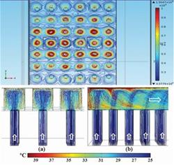
Micro-jet array impinging flow simulation.
   IME have complete assembly and packaging capabilities to offer solutions for 2.5D assembly using large & thin interposer, 3D Chip stacking using Chip-to-Wafer & Chip-to-Chip Bonding, FOWLP wafer reconstruction, power module packaging and photonics Packaging. We also offer assembly and packages services such as wafer thinning, wafer sawing, wafer level compression molding, flip chip bonding using mass reflow & thermal compression bonding, solder ball attachment, wire bonding, etc.
IME have reliability test capabilities such as Temperature Cycle Test, High Temperature Storage Test (HTS),  Moisture Sensitivity Level Test (MSL), un-biased Highly Accelerated Stress Test (un-biased HAST), Drop Test and etc, which can support component level and board level testing. We also have complete failure analysis capabilities such as SEM, TEM, FIB, CSAM, X-ray etc. IME also offer reliability testing and failure analysis services. 

Advanced Packaging Design

IME advanced packaging program offer package architecture design solutions for new products together with Electrical, Thermo-Mechanical and Thermal modelling & simulations for overall package performance in terms of electrical, thermal and reliability.
Electrical Modelling 


Electrical modelling and simulations 

  • Antenna design for 5G and automotive radar applications
  • RLC parametric extraction, Signal & Power Integrity
  • EDA/ PDK reference flow for various packaging technologies
  • Electrical characterization tools

Mechanical Modelling 

Mechanical Modelling and Simulations

  • Package parametric study
  • Wafer level & package level warpage
  • Mold flow and die shift
  • Solder joint fatigue under TC and drop test conditions
  • Material characterization capabilities

Thermal Modelling 


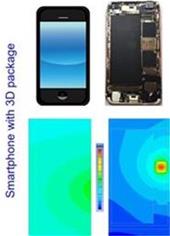
Thermal modelling and Simulation

  • Active and Passive thermal solutions
  • Board Level Thermal Performance characterization