Heterogeneous Integration

Heterogeneous Integration (HI) group uses advanced packaging platforms to integrate devices in order to solve Moore's law-predicted scaling issues. In order to maintain and further enhance progress, HI is essential for higher performance, lower latency, smaller form factors, lighter weight, less power requirement per function, and lower cost. Targeted end applications include mobile, 5G, data centres, automotive, IOT etc. 

In IME, we can provide system level packaging solutions to industry partners via R&D pilot runs, service jobs, small-volume production, and technology transfer through our state-of-the-art 300mm Advanced Packaging Development line and Assembly lab.

Fan-out Wafer Level Packaging (FOWLP) for Automotive mmWave Antenna-in-Package

FOWLP

There are increasing technology demand in the automotive industry for Advanced driver-assistance systems (ADAS) for Adaptive Cruise Control, Lane Change Assist, Automatic Emergency Brake and Forward Collision Avoidance etc. ADAS relies on inputs from multiple systems, such as automotive imaging, LiDAR, V2V/V2X communication and RADAR.
Currently the industry has widely adopted 77Ghz for the RADAR frequency for 30 to 250 meters range and 79GHz shall be adopted by the industries for mid to short range detection. To ensure reliable and high performance for the 77GHz/79GHz RADAR at millimetre wavelength, IME proposes the use of Fan-Out Wafer Level Packaging (FOWLP) which has several key advantages such as low dielectric loss, shorter interconnects length, excellent impedance matching, higher Q inductance, significant reduction in cost/size and many more.

Fan-out Wafer Level Packaging (FOWLP) for 5G mmWave Antenna-in-Package

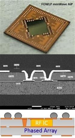
Antena-in-Package Cross section of FOWLP mmWave AiP.   5G base stations require proper integration of the Power Amplifier (PA) chips,  millimetre wave monolithic ICs (MMIC), passive components and millimetre wave (mmWave) antenna array to support high speed and large bandwidth communication. However, to ensure lower electrical losses,  tighter process controls are required to ensure proper matching as a manufacturing requirement to the 5G base station modules. 
To tackle these issues, IME proposes the use of Fan-Out Wafer Level Packaging (FOWLP) which allows 3D integration of the mmWave phase array antennas on top of the RF ICs within a single package. This allows components to be closely connected and ensure minimum interconnection losses. Wafer level packaging shall be used to further reduce parasitic losses and ensure adequate impedance matching. 3D FOWLP integration further allows a scalable sub-array AiP to be formed which subsequently is then used to realize the larger antenna array. 

Wafer Level Packaging

Fan-out Wafer Level Packaging (FOWLP) for 5G mmWave Antenna-in-Package

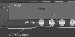
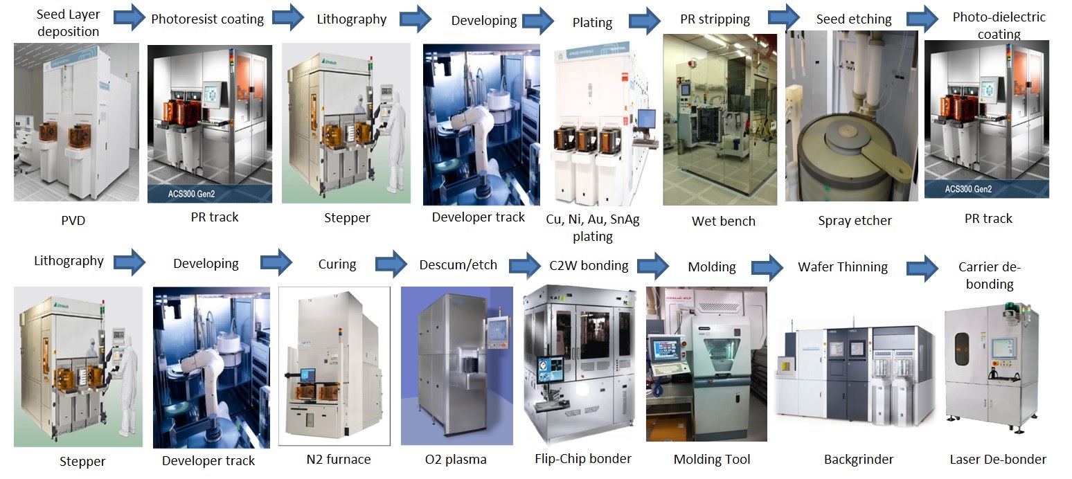
IME has state of the art 300mm advanced wafer level packaging engineering line which can support various advanced wafer level packaging technologies development such as Mold-First and RDL-First FOWLP, Passive and Active Interposers for 2.5D and Via-Middle & Via-Last TSV integration for 3D IC packaging etc used in mobile, AI, Data Centre and IoT applications. IME offer end-to-end solutions in FOWLP & 2.5D/3D packaging and shorten the development cycle time for new applications. We also offer services in the area of wafer level fine pitch RDL of 2um/2um LW/LS, C4 solder bumping & Cu pillar micro bumping up to 20um pitch, temporary bonding & de-bonding, TSV fabrication etc.

IME Multi-Chip 12" FOWLP Development Line

Wafer Level Packaging Line

TSV, 2.5D INTERPOSER AND 3DIC INTEGRATION

IME offers a variety of TSV processes like TSV backside reveal, Via-Middle, Via-Last TSVs fabrication.  We have state-of-the-art advanced packaging tools to support TSV aspect ratio of up to 20:1. Depending on the requirement, via-last TSV can be implemented from either the frontside or backside of the wafer.


We can fabricate interposer on a variety of substrates (Si, high-resistive Si, SOI) for different 2.5D heterogeneous integration applications. Fine-pitch Cu damascene metal lines of up to 4 layers for routing can be supported on the interposer frontside with 1 layer of Cu RDL on interposer backside.
To enable 3D-IC stacking, in addition to TSVs and metallization, IME has also developed wafer-to-wafer, chip-to-wafer fusion and hybrid bonding processes for different applications like memory stacking, high-performance compute.  Bonding accuracy of 0.5m can be achieved.


CRYOGENIC PACKAGING FOR QUANTUM TECHNOLOGIES

IME also provides packaging solutions for quantum technologies. For reduction in loss and heat dissipation, superconducting metallization and TSVs can be implemented on 2.5D interposers for operation in cryogenic temperatures. Integrated waveguides can also be embedded in the packages for form factor and control of qubits.