NEW Fabrication & Packaging Services banner

R&D Foundry

Wafer Fabrication Services

The Institute of Microelectronics (IME) offers a broad range of services to our customers to meet the research and development (R&D) needs of the semiconductor and related industries.

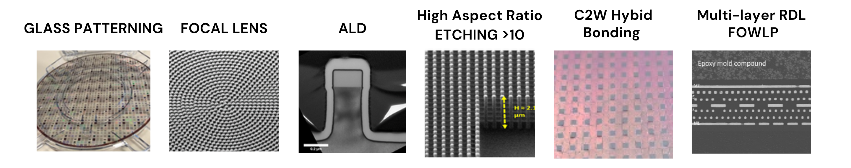
IME’s Fab is located in-house and provides R&D services related to advanced packaging, piezo MEMS, photonics and flat optics, wide bandgap semiconductors, and Medtech applications. IME is equipped with industry-standard 200 mm and 300 mm wafer processing equipment in 3000 m2 of Class-10 cleanroom facilities, supported by metrology, assembly, material characterization and electrical characterization laboratories.

Wafer Fabrication Services

Lithography

  • GHI-line Steppers (>0.8 µm L/S)
  • ArF Immersion scanner (>45 nm L/S)

Physical Vapor Deposition

  • Ta/TaN Cu barrier seed
  • Al/ Ti / TiN

Chemical Vapor Deposition/Atomic Layer Deposition

  • Cu RDL, Cu pillar, Cu TSV, Cu damascene
  • UBM, SnAg bump

Electroplating (ECP)

  • Cu RDL, Cu pillar, Cu TSV, Cu damascene
  • UBM, SnAg bump

Bonding

  • Polymer/glue bonding
  • Fusion bonding
  • Hybrid bonding
  • Metal TCB/Eutectic bonding

Metrology

  • Macro & Micro Defect Review 
  • Defect Review SEM
  • Sidewall Roughness
  • Surface Morphology
  • Film Stress/ Warpage
  • Film Thickness measurements

Furnace

  • Anneal
  • Polymide , Dielectric Cure

Etch

  • Desdum
  • Silicon
  • Oxide
  • Silicon-Nitride

Customized Solutions

  • Specialty CVD/PVD depositions
  • New materials evaluations

Fab Services

IME offers advanced lithography services printing 45nm and above patterns for 300mm wafers using immersion lithography. Defect review capability for 30nm above pattern defects, surface defects, advanced overlay and CD measurement are also available.  

Lithography

  • 365nm Stepper
  • 193nm Immersion Scanner

Physical Vapor Deposition

  • Cu
  • Al 
  • Ti / TiN

Atomic Layer Deposition

  • HfO/ HfN
  • Al2O3

Chemical Vapor Deposition 

  • Silicon Nitride
  • Silicon Oxide

Bonding

  • Temporary / Permanent
  • Fusion
  • Polymer
  • Hybrid
  • Metal

Metrology

  • Macro & Micro Defect Review and Binning
  • Defect review SEM
  • Sidewall Roughness
  • Surface Morphology
  • Film Stress / Warpage
  • Thickness Measurements

Electroplating (ECP)

  • Cu Pillar, RDL, UBM
  • TSV Cu

Furnace

  • Anneal
  • Polymide, Dielectric Cure

Etch

  • Descum
  • Silicon
  • Oxide
  • Silicon-Nitride
  • Aluminium

Customized Solutions 

  • Specialty CVD / PVD Depositions
  • New Materials Evaluations
  • Deep Machines Learning Applications

Chemical and Mechanical Polish

  • Silicon oxide
  • Copper
  • Titanium

Material, Device, Reliability Analysis (MDRA)

Material Devices and Reliability Analysis (MDRA) has the capabilities and cutting-edge facilities to conduct world-class research and development in semiconductor technology. We provide materials and process characterization, failure analysis, and reliability testing to support our industry partners in wafer fabrication, packaging, assembly, and test.

12" Probe Station

  • Automated IV, CV measurements on 12" wafers

FEI Double beam FIB

  • Up to 65 nA Ga* beam current under 30KV
  • High resolution SEM/STEM imaging (0.6nm at 15KV)
  • In-situ TEM sample preparation

FE-SEM

  • High resolution SEM imaging with EBSD and EDX analysis (0.8nm at 15KV)

3D X-Ray

  • Nondestructive 3D X-Ray imaging
  • High spatial resolution to 500nm

Ar Ion Milling/Polisher

  • Sample preparation for SEM and optical microscope analysis

CSAM Sonix

  • Transducers from 15 KHz to 230MHz for C-Scan/T-Scan analysis
  • 12" warped wafer compensation

Thermal Shock Chamber

  • Test standard JESD22-A104
  • Temperature range (-70°C to 300°C)

Thermal Humidity Chamber

  • Test standard JESD22-A101
  • Temperature stress: 85°C & relative humidity stress: 85%

ESD Tester

  • MM/HBM Test

High temperature storage chamber

  • Test standard JESD22-A103
  • Temperature storage up to 300°C

Thermal Shock  (liquid to liquid)

  • Test standard JESD22-A106
  • Temperature range (-65°C to 200°C)

FEI TEM (CM200)

  • 200KV transmission electron beam analysis (resolution < 0.14nm)

FAB Capabilities

Etch

  • Etching processes on 200 and 300 mm wafers
  • Cavities with depth up to 500 µm
  • Vias and trenches with depth up to 100 µm, aspect ratio ≥ 10:1
  • Silicon and SiN pillars with minimal dimensions of 60nm
  • SiO2 and SiN based dielectrics of different thicknesses and critical dimensions with controllable sidewall angle
  • Metal etch

Lithography

  • Capable of 45nm line/space resolution
  • Advanced Packaging applications, capable of 1um resolution, 200mm & 300mm thinned and warped wafer handling
  • 200mm i-line stepper for MEMS applications, capable of 0.5um resolution with front to back alignment

In-Line Metrology

  • 8” or 12” Metrology measurement services available for Defect Review, Defect Binning, Particle count, Film Thickness (Metal / Non-Metal) and Critical Dimension measurement
  • Atomic Force for surface roughness measurement
  • TSV Metrology

Thin Film

  • Physical vapour deposition (PVD), chemical vapour deposition (CVD), atomic layer deposition (ALD) and electroplating (ECP) services available 
  • Silicon wafers bonding service is also available for 12” and 8” wafers