Edge computing group partners with research institutes and local universities to foster multidisciplinary, high-impact research via exploiting both architecture and circuit techniques to enhance the computation efficiency for domain specific applications.
We focus on three main research areas:
Hardware accelerator: We tackle enormous data flow and computation workloads of domain-specific tasks via unorthodox approaches: (1) Tailored processing engine (PE) design (2)
Novel memory & In-memory computing circuits (3) Data-driven energy-enhancement techniques.
Low-power RISC-V: We explore open-source RISC-V architecture as a platform to enable innovation in Edge AI. Our first RISC-V chip has been fabricated and tested in 40nm CMOS and we are expanding our custom instructions and silicon
fabrics to harvest the full potential of our hardware accelerators (Fig. 1)
Cryogenic circuits for quantum technologies: We provide energy-efficient and high-speed IPs that enable large-scale quantum computing for the future. On top of conventional
AISC design and verification methodology, these circuits require specific modelling, compensation, and test set-up so that they are able to operate down to 4K temperature (Fig. 2).
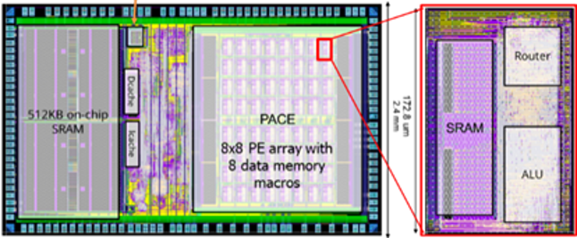
Fig.
1 RISC-V processor with 512kB on-chip memory & coarse-grain reconfigurable
PE array | 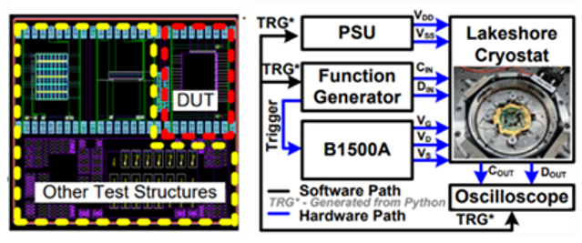
Fig.
2 Cryogenic CMOS test chip and cryogenic measurement set-up |