Electronics & Photonics
IHPC drives the innovation in electronics and photonics through computational technologies. The three main research areas are:
- Nano & Quantum Photonics/AI
- Electromagnetics
- 3D Inverse Imaging & Optical Modelling
Nano & Quantum Photonics/AI
IHPC drives the photonics innovation through computational technologies thanks to the development of nanoscale physical optics-based approaches for theory, modelling, simulation, design and optimisation of optical structures, devices and systems.
We synergise the efforts across low loss quantum photonics platforms, nano- & quantum-plasmonics, resonant nanophotonics, metasurfaces and physics-based AI assisting light-matter interaction to develop key capabilities and translate into impactful applications including quantum technologies, Datacom, medical technology, IoT sensors, energy and lighting.
Our mission is to advance science and engineering technologies for generating, controlling, transmitting and processing properties of light-matter based on the multi-scale, multi-physics and multi-disciplinary computational tools.
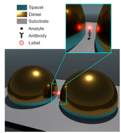
Schematic illustration of the strong coupling of quantum plasmonic immunoassay sensing
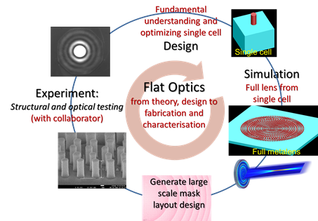
Flat Optics from design, modelling & simulation to experiment
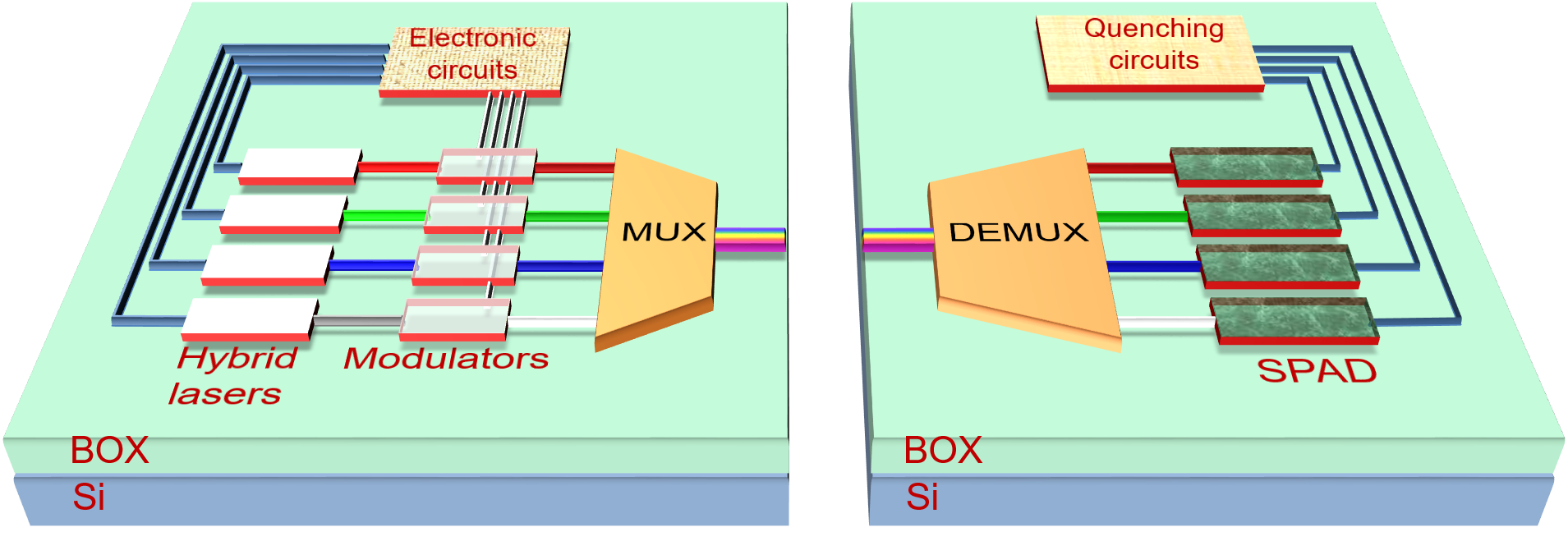 Illustration of proposed quantum photonic integrated circuit
Electromagnetics
The requirement of eco-environment and expectation of future technology stimulate and promote the rapid development in electromagnetics and wireless technologies. Through internal in-depth research and external collaboration with industry, universities and government agencies in many years, robust expertise and solid capabilities in electromagnetics and wireless technologies have been developed, i.e.
- Computational electromagnetic algorithms and modelling methods,
- Chip/board/system-level electromagnetic interference and compatibility (EMI/EMC),
- Electrostatic discharge (ESD), Lightning,
- Electromagnetic shielding, high frequency filtering,
- Electromagnetic environment effect,
- Wireless energy transfer,
- Wireless signal propagation and strength optimisation,
- Antenna and RFID.
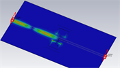
Defected ground structure based common-mode filter
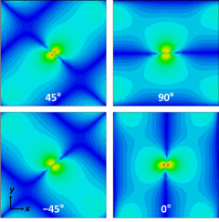
Electric current distribution on each ply of an aircraft CFRP composite
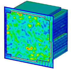
Electromagnetic field distribution in a communication system
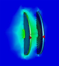
Field coupling between transmitter and receiver of a wireless charging system
3D inverse imaging & optical modelling
IHPC develops advanced algorithms and models for non-destructive testing (NDT), spanning from magnetic, eddy current, microwave imaging to THz, X-ray, and optical imaging. Our unique capability in 3D Inverse Imaging is applicable for not only detecting the locations of defects in structures- and components-under-test, but also quantifying and characterising the shape and size of defects via advanced inversion and imaging algorithms. This technology will provide more holistic decision makings and help rely less on skill sets and expertise.
For the Optical Modelling, we develop fast algorithms using ray optics for light transport to address the modelling and simulation needs of different domains and industry sectors. Besides the typical applications in micro-optics design for the electronics industry, computational ray optics methodologies have been applied to laser-assisted additive manufacturing systems, wireless & LiFi communications for aerospace, building environment, indoor daylighting and artificial lighting for AgriTech, outdoor solar and radiant thermal comfort at the city-scale.
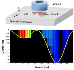
Modelling and imaging of surface-breaking cracks using eddy current scanning
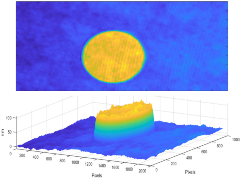
Optical interferometry diffraction phase microscopy - 3D reconstruction of 60µm diameter, 100nm high SiO2 pillars on Si wafer

Solving inverse scattering problems against experimental data from Institut Frenel on the example FoamTwinDiel at 10 GHz - (a) original profile, (b), (c), and (d) three steps of inversions, where imaging results are getting finer and more accurate
A*STAR celebrates International Women's Day

From groundbreaking discoveries to cutting-edge research, our researchers are empowering the next generation of female science, technology, engineering and mathematics (STEM) leaders.
Get inspired by our #WomeninSTEM
.png?sfvrsn=ff199933_15)