.png?sfvrsn=ff199933_15)
Manufacturing & Engineering
- Health & Human Potential
- Manufacturing & Engineering
- Smart Nation & Digital Economy
- Transport & Connectivity
- Urban Solutions & Sustainability
Pad Conditioning Simulation Platform
The high cost of semiconductor chips is primarily driven by manufacturing costs. Chemical mechanical planarisation (CMP) or polishing is critical to polish IC layers on silicon wafers to ensure chip quality and accounts for about 7% of the cost in semiconductor manufacturing.
In typical CMP (Fig 1.), the wafer is mounted on a rotating carrier and pressed against a pad affixed to a rotating plate. The CMP pad needs to be conditioned continuously to ensure it has appropriate surface characteristics. The conditioning process significantly affects the pad surface quality and service life, and thus tuning the conditioning parameters is a crucial step in chip manufacturing.
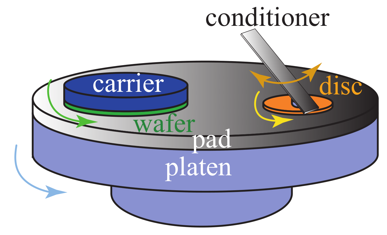
Fig 1. Schematic of a CMP process [1]
The pad conditioning simulation platform developed in this work is to model the conditioning process and thus significantly reduce process and product design cycle time, typically determined with expensive experimental tests.
Features
- Flexibility in choosing different disc designs with different diamond distributions
- Pad conditioning simulation capability over long time process circles
- Conditioning density distribution estimation after multiple conditioning steps with different conditioning parameters
- Flexibility in defining different sweep motions for the conditioner arm
- Enables estimation of optimal
The Science Behind
The conditioning process comprises a relatively complicated kinematic system (Fig 2.) that includes the rotation of the pad and disc and the sweep motion of the conditioner arm. At different stages, the steps are defined with altered kinematic parameters. Moreover, there are typically several hundred diamond tips (illustrated in Fig 3.) mounted on the disc, which control the polishing rate and need to be individually tracked during the entire process.
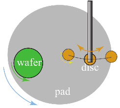
Fig 2. Kinematic involved
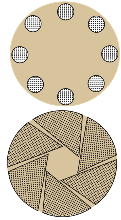 Fig 3. Disc Design [2]
It imposes significant computational effort with small time-step size to cope with the large variance of relative speeds of the different diamond feature tips. With a novel trajectory tracing algorithm and a user-friendly GUI system, the platform can produce the conditioning density distribution map under different conditioning settings.
Industry Applications
- Semiconductor manufacturing (CMP process)
- Product design (conditioning disc design)
- [1] Li, et.al., Precision engineering, 2012, 36(2): 356-363
- [2] Baisie, et.al., The International Journal of Advanced Manufacturing Technology 66 (2013) 2041–2052
For more info or collaboration opportunities, please write to enquiry@ihpc.a-star.edu.sg.
A*STAR celebrates International Women's Day

From groundbreaking discoveries to cutting-edge research, our researchers are empowering the next generation of female science, technology, engineering and mathematics (STEM) leaders.
Get inspired by our #WomeninSTEM