- Press Releases
- Industry Updates
- SIMTech Manufacturing Matters
- Manufacturing Matters
- SIMTech 30th Anniversary
- Events
- ASPEN2022
- BCA Green Mark (Platinum) for Healthier Workplaces and Laboratories
Picosecond Laser Micromachining of Tungsten Carbide
Cost-effective and flexible method to machine high-quality microfeatures and patterns

Tungsten carbide (WC) is a widely used tool material in industry due to its unique properties such as high hardness, excellent wear resistance, chemical inertness, and dimensional stability. However, it is also known to be a
difficult-to-machine material. Due to its toughness and hardness, conventional mechanical machining methods such as electrical discharge machining (EDM) and grinding may encounter problems like tool wear, easy breakage of tool, and it
is also time-consuming.
Through this method, we can now drill high-quality microholes, engrave various features, and produce micro/nano surface structures on a tungsten carbide surface
As such, an alternative cost-effective and high efficiency machining method is needed. Laser micromachining is one promising option with its unique properties such as noncontact processing, no mechanical cutting forces, and no process
tool wear. However, use of conventional lasers such as the nanosecond pulsed laser to machine tungsten carbide has been found to cause thermal effects and residual material redeposition issues due to cemented WC’s composite material
properties.
An efficient picosecond pulsed-laser WC micromachining process has been developed.
Compared to conventional EDM techniques, the picosecond laser WC micromachining process is efficient in terms of shorter machining time and flexibility. With properties such as ultrashort pulse duration and high peak-power intensity,
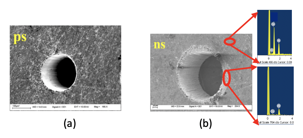
the picosecond pulsed laser produces results much different from those of conventional lasers (Fig 1). A major advantage of ultrashort lasers is their ability to generate high peak power and deliver energy into a material rapidly before
thermal diffusion occurs. During ultrashort pulsed laser processing, material is removed mainly by vaporisation. In addition, the laser-irradiation-induced heat-affected zone (HAZ) and molten material are significantly reduced due to
the ultrashort pulse duration.

Figure 1: Ultrashort picosecond laser drilled hole (a) and conventional nanosecond laser drilled hole (b) on WC substrates
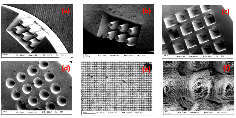
As illustrated in Fig 2, a picosecond laser is able to drill through WC substrates with different thicknesses up to 0.5 mm thick and a hole size range of 50 to 250 µm, to engrave high-quality different shaped features with an aspect
ratio of 4.5. Furthermore, such method is able to fabricate two-scale hierarchical micro/nano microbump-based surface textures on WC substrates to have a lotus-leaf-like hydrophobic surface. All of which would improve the performance of
the fabricated WC-based moulds, dies and tools.
In recognition of its scientific novelty and potential applications, the work has been highlighted in the global coverage magazine INDUSTRIAL LASER SOLUTIONS as a Technology Report.

Figure 2: Picosecond laser engraved square and circular-shaped miro-pillars (a) & (b), micro-cavities (c) & (d) and 2 scale micro/nano hierarchical micro-bump array surface structures (e) & (f) on WC substrates
A*STAR celebrates International Women's Day

From groundbreaking discoveries to cutting-edge research, our researchers are empowering the next generation of female science, technology, engineering and mathematics (STEM) leaders.
Get inspired by our #WomeninSTEM
.png?sfvrsn=843a4005_8)