Advanced Packaging
Advanced packaging at IME is driven by the needs of local & global industry partners to design, demonstrate and prototype novel packages to meet market requirements in hyper-scale data centres, AI, 5G and automotive applications.
Through Advanced packaging, IME integrates heterogeneous chiplets to provide power, performance, form factor, cost optimised System-in-Package solutions such as wafer level Package-on-Package, 3D stacked memory, Antenna-in-package, co-packed optics and intelligent power modules.
IME’s heterogeneous integration pilot line allows diverse chiplets to be integrated into state-of-the-art advanced packages. Our technologies include high-density Fan-out-Wafer-Level Packaging (FOWLP), 2.5D interposers, 3D TSV, Chip-to-Wafer (C2W)/ Wafer-to-Wafer (W2W) hybrid bonding.
IME’s system-in-package designs are realized by our verified PDKs and optimized through accurate multi-physics modelling to produce packages that have strong mechanical, thermal, and electrical integrity.
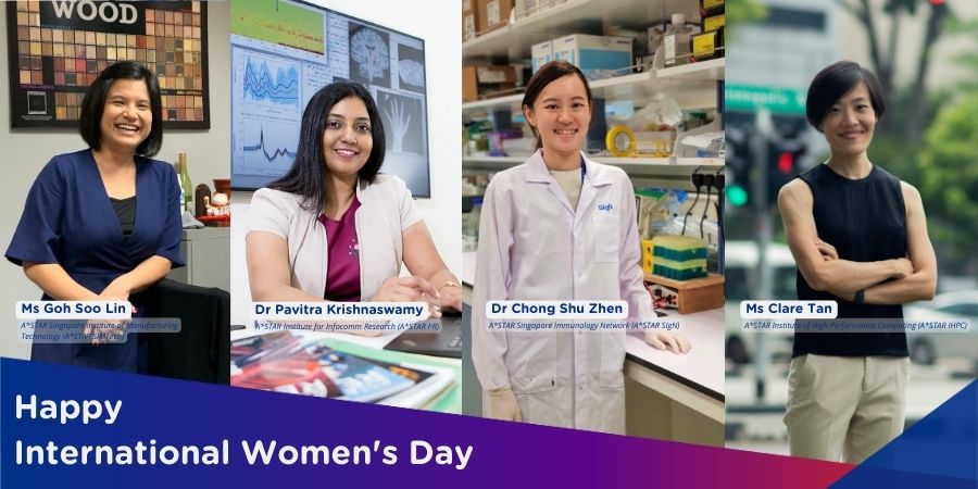
A*STAR celebrates International Women's Day

From groundbreaking discoveries to cutting-edge research, our researchers are empowering the next generation of female science, technology, engineering and mathematics (STEM) leaders.
Get inspired by our #WomeninSTEM
