Research In SIMTech
Surface Technology Group (STG)
Introduction
Surface modification and coating technologies are widely used to augment product surface functions and improve the performance of components and systems. With the advancement in materials and manufacturing processes, surface technology plays a crucial role in realising new engineering breakthroughs and performance
enhancements in various fields.
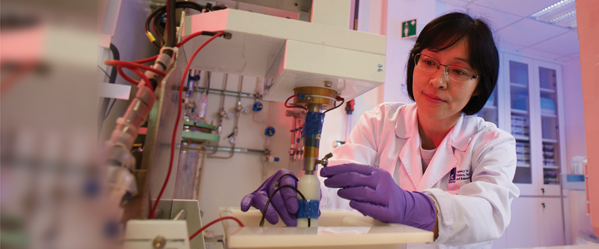
The Surface Technology (STG) group focuses on hybrid tribological composite and multi-functional coatings, surface modification, and nanostructures through materials synthesis, coating design, process innovation, and customisation for a wide range of applications. The group carries out collaborative research with academic institutions and co-develops processes and products with companies, while providing technology transfer and training to the manufacturing industry.
Research Themes
- Electrochemical Process
The Electrochemical Process Team works on the development and application of various aqueous solution-based electrochemical processes, including electroplating, electroless plating, anodising, and high-precision electroforming. The areas that the team can effectively engage with the local industry are electrochemical processes for coatings, waste treatment, as well as micro/nano-structuring. - Functional Coatings
The Functional Coating Team works on wet chemical coating formulation and processes, and chemical synthesis of nanomaterials to add functions into coatings. The application areas of the functional coatings include precision engineering, appliances, optoelectronic devices, biomedical components, building and construction, aerospace, automotive, and more. The substrates include metals, glass, ceramics, all polymers, and textiles. - Vapour Deposition
The Vapour Deposition and Thermal Spray Team has been working in the field of tribological and corrosion protective coatings to prolong the lifetime or enhance the surface function or performance of industrial tools and wear components. The team has established core competence and expertise in coating deposition processes and materials engineering pertaining to the application conditions and performance requirements for surface wear or corrosion protection, and other functions such as dry lubrication or anti-sticking.
Core Competencies
- Electrochemical Processes
- Electroless and electrolytic coatings
- Metallisation of non-conductive substrates
- Anodising and Plasma Electrolytic Oxidation (PEO)
- Electropolishing
- Physical Deposition Processes
- Customised PVD coating design and engineering
- PVD Coating material and processes
- Thermal spray and HVOF processes
- Hybrid Surface Treatments and Coatings
- Thin film device design and fabrication
- Micro/Nano surface patterning and texturing
- Electroforming and photochemical etching
Technologies for Licensing and Transfer
- Electrochemical Processes
- Rapid deposition of high-phosphorus nickel alloy coating for diamond turning
- Metallisation of PEI polymers and composites
- Metallisation of HDPE polymers
- Metallisation of MgO-based ceramics
- Plasma electrolytic oxidation of light metals
- Green lacquer stripper for effective removal of organic coatings from high-precision metal components
- Physical Deposition Processes
- Hard coatings for cutting tools
- Decorative coatings with different colours
- Anti-stick coating for IC packaging & plastic injection moulding processes
- Conductive nanocomposite coatings for electrical contact applications
- Hard chrome replacement by plasma spray ceramic coatings for hydraulic cylinders
- HVOF WC coatings for wear resistance
- Hybrid Surface Treatment and Coatings
- Photo electro and chemical etching for surface micro/nano texturing and high precision components
- Air plasma-based surface treatments and ultrathin coatings
Key Achievements
- USA Patent Application No. 15/780,063, “Method of Purifying Nanostructures”, Filing date: 30 May 2018
- International Patent No. WO2017098207A1, “Methods of Purifying Nanostructures”, Publication date: 15 June 2017
- China Patent, CN108367346, “纯化纳米结构的方法”, Filed on 29 November 2016.
- International Patent No. WO2015137878A1, Filter devices and filtering methods, Publication date: 17 September 2016
- SG Provisional Patent Application No.: IPOS10201601817P, “High Phosphorus Nickel Alloy Coatings by Electrolytic Plating for Diamond Turning”, Filed on 9 March 2016
- UK patent application No. 1521581.7: “Method of Purifying Nanostructures”, Filing date: 08 Dec 2016
Listing of Some Major Equipment
- Electrochemical Process
- Anodising pilot line
- Electro/Electroless plating pilot lines
- Brush plating system
- Rapid plating system
- Photo-chemical etching system
- Functional Coatings
- Particle analysis systems (ZetaSizer, Nanosight)
- Automated Reactors
- Coating Process Systems (Inkjet, Spray booth, Dip coater)
- Dynamic and static contact angle goniometer
- Agitator Bead Mill
- Vapour Deposition
- Plasma Enhanced Physical Vapour Deposition System
- Platit Cathodic Arc Deposition System
- Unbalanced Magnetron Sputtering Physical Vapour Deposition System
- CemeCon HIPIMS Physical Vapour Deposition System
- E-beam Physical Vapour Deposition System